- 您现在的位置:买卖IC网 > PDF目录373901 > AD7490BCP (ANALOG DEVICES INC) 16-Channel, 1 MSPS, 12-Bit ADC with Sequencer in 28-Lead TSSOP PDF资料下载
参数资料
| 型号: | AD7490BCP |
| 厂商: | ANALOG DEVICES INC |
| 元件分类: | ADC |
| 英文描述: | 16-Channel, 1 MSPS, 12-Bit ADC with Sequencer in 28-Lead TSSOP |
| 中文描述: | 16-CH 12-BIT SUCCESSIVE APPROXIMATION ADC, SERIAL ACCESS, QCC32 |
| 封装: | MO-220-VHHD-2, LFCSP-32 |
| 文件页数: | 13/24页 |
| 文件大小: | 2255K |
| 代理商: | AD7490BCP |
AD7490
–13–
REV. A
the on resistance of a switch (track and hold switch) and also includes
the on resistance of the input multiplexer. The total resistance is
typically about 400
. The capacitor C2 is the ADC sampling
capacitor and typically has a capacitance of 30 pF. For ac appli-
cations, removing high frequency components from the analog
input signal is recommended by use of an RC low-pass filter on
the relevant analog input pin. In applications where harmonic distor-
tion and signal-to-noise ratio are critical, the analog input should
be driven from a low impedance source. Large source impedances
will significantly affect the ac performance of the ADC. This
may necessitate the use of an input buffer amplifier. The choice
of the op amp will be a function of the particular application.
When no amplifier is used to drive the analog input, the source
impedance should be limited to low values. The maximum
source impedance will depend on the amount of total harmonic
distortion (THD) that can be tolerated. The THD will increase as
the source impedance increases, and performance will degrade
(see TPC 5).
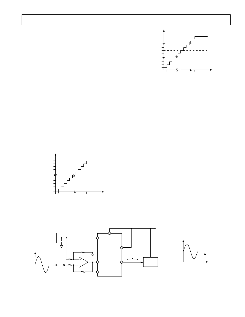
ADC TRANSFER FUNCTION
The output coding of the AD7490 is either straight binary or twos
complement depending on the status of the LSB (RANGE Bit) in
the Control Register. The designed code transitions occur midway
between successive LSB values (i.e., 1 LSB, 2 LSBs, and so on).
The LSB size is equal to REF
IN
/4096. The ideal transfer charac-
teristic for the AD7490 when straight binary coding is selected
is shown in Figure 8.
000…000
0V
ANALOG INPUT
111…111
111…110
000…001
000…010
111…000
011…111
1 LSB
+V
REF
1 LSB
1 LSB V
REF
/4096
V
REF
IS EITHER REF
IN
OR 2 REF
IN
Figure 8. Straight Binary Transfer Characteristic
V
REF
R3
R2
R4
R1
REF
IN
V
IN
0
V
IN
15
AD7490
DSP/ P
V
DD
0.1 F
V
V
DD
V
DRIVE
DOUT
TWOS
COMPLEMENT
+REF
IN
( 2 REF
IN
)
REF
IN
–REF
IN
( 0V)
011…111
000…000
100…000
0V
V
R1 R2 R3 R4
Figure 10. Handling Bipolar Signals
–V
REF
1 LSB
A
ANALOG INPUT
+V
REF
1 LSB
1 LSB 2 V
REF
4096
V
REF
1 LSB
100…000
011…111
011…110
100…001
100…010
000…001
000…000
111…111
Figure 9. Twos Complement Transfer Characteristic
with REF
IN
±
REF
IN
Input Range
Handling Bipolar Input Signals
Figure 10 shows how useful the combination of the 2 REF
IN
input range and the twos complement output coding scheme is for
handling bipolar input signals. If the bipolar input signal is biased
about REF
IN
and twos complement output coding is selected,
then REF
IN
becomes the zero code point,
–
REF
IN
is negative
fullscale and +REF
IN
becomes positive full scale, with a dynamic
range of 2 REF
IN
.
TYPICAL CONNECTION DIAGRAM
Figure 11
shows a typical connection diagram for the AD7490. In
this setup, the AGND pin is connected to the analog ground plane
of the system. In Figure 11, REF
IN
is connected to a decoupled
2.5 V supply from a reference source, the AD780, to provide an
analog input range of 0 V to 2.5 V (if RANGE Bit is 1) or 0 V to
5 V (if RANGE Bit is 0). Although the AD7490 is connected to a
V
DD
of 5 V, the serial interface is connected to a 3 V micropro-
cessor. The V
DRIVE
pin of the AD7490 is connected to the same
3 V supply of the microprocessor to allow a 3 V logic interface
(see Digital Inputs section.) The conversion result is output in a
16-bit word. This 16-bit data stream consists of four address bits
indicating which channel the conversion result corresponds to,
followed by the 12 bits of conversion data. For applications where
相关PDF资料 |
PDF描述 |
|---|---|
| AD7490BRU | 16-Channel, 1 MSPS, 12-Bit ADC with Sequencer in 28-Lead TSSOP |
| AD7492 | Evaluation Board for 12-bit high speed, low power, successive-approximation ADC |
| AD7492CB | Evaluation Board for 12-bit high speed, low power, successive-approximation ADC |
| AD75004 | Quad 12-Bit D/A Converter |
| AD75004KN | ECONOLINE: REC2.2-S_DRW(Z)/H* - 2.2W DIP Package- 1kVDC Isolation- Regulated Output- 4.5-9V, 9-18V, 18-36V, 36-72V Wide Input Range 2 : 1- UL94V-0 Package Material- Continuous Short Circiut Protection- Cost Effective- 100% Burned In- Efficiency to 84% |
相关代理商/技术参数 |
参数描述 |
|---|---|
| AD7490BCP-REEL | 制造商:Analog Devices 功能描述:ADC Single SAR 1Msps 12-bit Serial 32-Pin LFCSP EP T/R |
| AD7490BCP-REEL7 | 制造商:Analog Devices 功能描述:ADC Single SAR 1Msps 12-bit Serial 32-Pin LFCSP EP T/R |
| AD7490BCPZ | 功能描述:IC ADC 12BIT 16CH 32-LFCSP RoHS:是 类别:集成电路 (IC) >> 数据采集 - 模数转换器 系列:- 标准包装:1 系列:microPOWER™ 位数:8 采样率(每秒):1M 数据接口:串行,SPI? 转换器数目:1 功率耗散(最大):- 电压电源:模拟和数字 工作温度:-40°C ~ 125°C 安装类型:表面贴装 封装/外壳:24-VFQFN 裸露焊盘 供应商设备封装:24-VQFN 裸露焊盘(4x4) 包装:Digi-Reel® 输入数目和类型:8 个单端,单极 产品目录页面:892 (CN2011-ZH PDF) 其它名称:296-25851-6 |
| AD7490BCPZ | 制造商:Analog Devices 功能描述:IC, ADC, 12BIT, 1MSPS, LFCSP-32 |
| AD7490BCPZ-REEL7 | 功能描述:IC ADC 12BIT 16CHAN 32LFCSP RoHS:是 类别:集成电路 (IC) >> 数据采集 - 模数转换器 系列:- 标准包装:1,000 系列:- 位数:16 采样率(每秒):45k 数据接口:串行 转换器数目:2 功率耗散(最大):315mW 电压电源:模拟和数字 工作温度:0°C ~ 70°C 安装类型:表面贴装 封装/外壳:28-SOIC(0.295",7.50mm 宽) 供应商设备封装:28-SOIC W 包装:带卷 (TR) 输入数目和类型:2 个单端,单极 |
发布紧急采购,3分钟左右您将得到回复。