- 您现在的位置:买卖IC网 > PDF目录10255 > AD7492ARUZ-4REEL7 (Analog Devices Inc)IC ADC 12BIT REF/CLOCK 24TSSOP PDF资料下载
参数资料
| 型号: | AD7492ARUZ-4REEL7 |
| 厂商: | Analog Devices Inc |
| 文件页数: | 6/24页 |
| 文件大小: | 0K |
| 描述: | IC ADC 12BIT REF/CLOCK 24TSSOP |
| 标准包装: | 1,000 |
| 位数: | 12 |
| 采样率(每秒): | 1.25M |
| 数据接口: | 并联 |
| 转换器数目: | 1 |
| 功率耗散(最大): | 16.5mW |
| 电压电源: | 模拟和数字 |
| 工作温度: | -40°C ~ 85°C |
| 安装类型: | 表面贴装 |
| 封装/外壳: | 24-TSSOP(0.173",4.40mm 宽) |
| 供应商设备封装: | 24-TSSOP |
| 包装: | 带卷 (TR) |
| 输入数目和类型: | 1 个单端,单极 |
| 配用: | EVAL-AD7492CBZ-ND - BOARD EVALUATION FOR AD7492 |
AD7492
Rev. A | Page 14 of 24
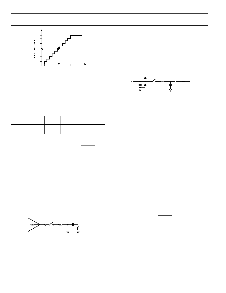
111...111
111...110
111...000
011...111
000...010
000...001
000...000
A
DC
CO
DE
ANALOG INPUT
1LSB = VREF/4096
0V 1/2LSB
+VREF –1LSB
01
12
8-
01
6
Figure 16. Transfer Characteristic for 12 Bits
AC ACQUISITION TIME
In ac applications, it is recommended to always buffer analog
input signals. The source impedance of the drive circuitry must
be kept as low as possible to minimize the acquisition time of
the ADC. Large values of impedance at the VIN pin of the ADC
cause the THD to degrade at high input frequencies.
Table 6. Dynamic Performance Specifications
Input
Buffers
SNR
500 kHz
THD
500 kHz
Typical Amplifier Current
Consumption
69.5
80
17 mA
69.6
81.6
8.2 mA
DC ACQUISITION TIME
The ADC starts a new acquisition phase at the end of a
conversion and ends it on the falling edge of the CONVST
signal. At the end of the conversion, there is a settling time
associated with the sampling circuit. This settling time lasts
120 ns. The analog signal on VIN is also acquired during this
settling time; therefore, the minimum acquisition time needed
is 120 ns.
Figure 17 shows the equivalent charging circuit for the sampling
capacitor when the ADC is in its acquisition phase. R3
represents the source impedance of a buffer amplifier or
resistive network, R1 is an internal switch resistance, R2 is for
bandwidth control, and C1 is the sampling capacitor. C2 is
back-plate capacitance and switch parasitic capacitance.
During the acquisition phase the sampling capacitor must be
charged to within 0.5 LSB of its final value.
R3
VIN
R1
125
C1
22pF
C2
8pF
R2
636
0
11
28
-01
7
Figure 17. Equivalent Analog Input Circuit
ANALOG INPUT
Figure 18 shows the equivalent circuit of the analog input
structure of the AD7492. The two diodes, D1 and D2, provide
ESD protection for the analog inputs. The Capacitor C3 is
typically about 4 pF and can be primarily attributed to pin
capacitance. The Resistor R1 is an internal switch resistance.
This resistor is typically about 125 Ω. The Capacitor C1 is the
sampling capacitor while R2 is used for bandwidth control.
D1
D2
VDD
R1
125
C1
22pF
C2
8pF
R2
636
VIN
C3
4pF
01
12
8-
01
8
Figure 18. Equivalent Analog Input Circuit
PARALLEL INTERFACE
The parallel interface of the AD7492 is 12 bits wide. The output
data buffers are activated when both CS and RD are logic low. At
this point the contents of the data register are placed onto the data
bus. Figure 19 shows the timing diagram for the parallel port.
Figure 20 shows the timing diagram for the parallel port when
CS and RD are tied permanently low. In this setup, once the
BUSY line goes from high to low, the conversion process is
completed. The data is available on the output bus slightly
before the falling edge of BUSY.
Note that the data bus cannot change state while the A/D is
doing a conversion, as this would have a detrimental effect on
the conversion in progress. The data out lines go three-state
again when either the RD or CS line goes high. Thus the CS can
be tied low permanently, leaving the RD line to control
conversion result access. Please reference the VDRIVE section for
output voltage levels.
OPERATING MODES
The AD7492 has two possible modes of operation depending
on the state of the CONVST pulse at the end of a conversion,
Mode 1 and Mode 2.
Mode 1 (High-Speed Sampling)
In this mode of operation the CONVST pulse is brought high
before the end of conversion, that is, before BUSY goes low (see
Figure 20). If the CONVST pin is brought from high-to-low
while BUSY is high, the conversion is restarted. When
operating in this mode a new conversion should not be initiated
until 140 ns after BUSY goes low. This acquisition time allows
the track/hold circuit to accurately acquire the input signal. As
mentioned earlier, a read should not be done during a
conversion. This mode facilitates the fastest throughput times
for the AD7492.
相关PDF资料 |
PDF描述 |
|---|---|
| AD7492ARUZ-REEL | IC ADC 12BIT REF/CLOCK 24TSSOP |
| AD7492ARUZ-4REEL | IC ADC 12BIT REF/CLOCK 24TSSOP |
| 5282-6SG-3DC | CONN RCPT 6POS CABLE SKT |
| AD7492ARZ-REEL | IC ADC 12BIT W/REF W/CLK 24-SOIC |
| VI-J4X-MX-S | CONVERTER MOD DC/DC 5.2V 75W |
相关代理商/技术参数 |
参数描述 |
|---|---|
| AD7492ARUZ-4REEL71 | 制造商:AD 制造商全称:Analog Devices 功能描述:1.25 MSPS, 16 mW Internal REF and CLK, 12-Bit Parallel ADC |
| AD7492ARUZ-5 | 功能描述:IC ADC 12BIT REF/CLOCK 24TSSOP RoHS:是 类别:集成电路 (IC) >> 数据采集 - 模数转换器 系列:- 标准包装:1,000 系列:- 位数:12 采样率(每秒):300k 数据接口:并联 转换器数目:1 功率耗散(最大):75mW 电压电源:单电源 工作温度:0°C ~ 70°C 安装类型:表面贴装 封装/外壳:24-SOIC(0.295",7.50mm 宽) 供应商设备封装:24-SOIC 包装:带卷 (TR) 输入数目和类型:1 个单端,单极;1 个单端,双极 |
| AD7492ARUZ-51 | 制造商:AD 制造商全称:Analog Devices 功能描述:1.25 MSPS, 16 mW Internal REF and CLK, 12-Bit Parallel ADC |
| AD7492ARUZ-5-REEL | 功能描述:IC ADC 12BIT REF/CLOCK 24TSSOP RoHS:是 类别:集成电路 (IC) >> 数据采集 - 模数转换器 系列:- 标准包装:1,000 系列:- 位数:12 采样率(每秒):300k 数据接口:并联 转换器数目:1 功率耗散(最大):75mW 电压电源:单电源 工作温度:0°C ~ 70°C 安装类型:表面贴装 封装/外壳:24-SOIC(0.295",7.50mm 宽) 供应商设备封装:24-SOIC 包装:带卷 (TR) 输入数目和类型:1 个单端,单极;1 个单端,双极 |
| AD7492ARUZ-5-REEL1 | 制造商:AD 制造商全称:Analog Devices 功能描述:1.25 MSPS, 16 mW Internal REF and CLK, 12-Bit Parallel ADC |
发布紧急采购,3分钟左右您将得到回复。