- 您现在的位置:买卖IC网 > PDF目录10255 > AD7492ARUZ-REEL7 (Analog Devices Inc)IC ADC 12BIT REF/CLOCK 24TSSOP PDF资料下载
参数资料
| 型号: | AD7492ARUZ-REEL7 |
| 厂商: | Analog Devices Inc |
| 文件页数: | 10/24页 |
| 文件大小: | 0K |
| 描述: | IC ADC 12BIT REF/CLOCK 24TSSOP |
| 标准包装: | 1,000 |
| 位数: | 12 |
| 采样率(每秒): | 1M |
| 数据接口: | 并联 |
| 转换器数目: | 1 |
| 功率耗散(最大): | 16.5mW |
| 电压电源: | 模拟和数字 |
| 工作温度: | -40°C ~ 85°C |
| 安装类型: | 表面贴装 |
| 封装/外壳: | 24-TSSOP(0.173",4.40mm 宽) |
| 供应商设备封装: | 24-TSSOP |
| 包装: | 带卷 (TR) |
| 输入数目和类型: | 1 个单端,单极 |
| 配用: | EVAL-AD7492CBZ-ND - BOARD EVALUATION FOR AD7492 |
AD7492
Rev. A | Page 18 of 24
GROUNDING AND LAYOUT
The analog and digital power supplies are independent and
separately pinned out to minimize coupling between analog and
digital sections within the device. To complement the excellent
noise performance of the AD7492, it is imperative that care be
given to the PCB layout. Figure 28 shows a recommended
connection diagram for the AD7492.
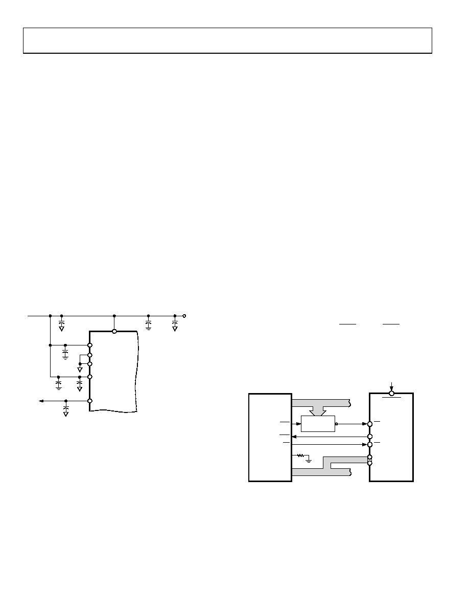
All of the AD7492 ground pins should be soldered directly to a
ground plane to minimize series inductance. The AVDD pin,
DVDD pin, and VDRIVE pin should be decoupled to both the
analog and digital ground planes. The REF OUT pin should be
decoupled to the analog ground plane with a minimum
capacitor value of 100 nF. This capacitor helps to stabilize the
internal reference circuit. The large value capacitors decouple
low frequency noise to analog ground, the small value
capacitors decouple high frequency noise to digital ground. All
digital circuitry power pins should be decoupled to the digital
ground plane. The use of ground planes can physically separate
sensitive analog components from the noisy digital system. The
two ground planes should be joined in only one place and
should not overlap so as to minimize capacitive coupling
between them. If the AD7492 is in a system where multiple
devices require AGND-to-DGND connections, the connection
should still be made at one point only, a star ground point,
established as close as possible to the AD7492.
AD7492
+
1nF
+
100nF
AGND
DGND
REF OUT
+
2.5V
ANALOG
SUPPLY
5V
47F
0.1F
10F
AVDD
DVDD
VDRIVE
01
12
8
-02
8
Figure 28. Typical Decoupling Circuit
Noise can be minimized by applying the following simple rules
to the PCB layout:
Analog signals should be kept away from digital signals.
Fast switching signals like clocks should be shielded with
digital ground to avoid radiating noise to other sections of
the board and clock signals should never be run near the
analog inputs.
Avoid running digital lines under the device as this couples
noise onto the die.
The power supply lines to the AD7492 should use as large a
trace as possible to provide a low impedance path and reduce
the effects of glitches on the power supply line.
Avoid crossover of digital and analog signals and place
traces that are on opposite sides of the board at right angles
to each other.
Noise to the analog power line can be further reduced by use of
multiple decoupling capacitors as shown in Figure 28.
Decoupling capacitors should be placed directly at the power
inlet to the PCB and also as close as possible to the power pins
of the AD7492. The same decoupling method should be used
on other ICs on the PCB, with the capacitor leads as short as
possible to minimize lead inductance.
POWER SUPPLIES
Separate power supplies for AVDD and DVDD are desirable, but if
necessary, DVDD can share its power connection to AVDD. The
digital supply (DVDD) must not exceed the analog supply (AVDD)
by more than 0.3 V in normal operation.
MICROPROCESSOR INTERFACING
ADSP-2185 to AD7492 Interface
Figure 29 shows a typical interface between the AD7492 and the
ADSP-2185. The ADSP-2185 processor can be used in one of
two memory modes, full memory mode and host mode. The
Mode C pin determines in which mode the processor works.
The interface in Figure 29 is set up to have the processor
working in full memory mode, allowing full external addressing
capabilities.
When the AD7492 has finished converting, the BUSY line
requests an interrupt through the IRQ2 pin. The IRQ2 interrupt
has to be set up in the interrupt control register as edge-
sensitive. The data memory select (DMS) pin latches in the
address of the ADC into the address decoder. The read
operation is started.
ADDRESS BUS
DATA BUS
100k
1ADDITIONAL PINS OMITTED FOR CLARITY.
OPTIONAL
ADDRESS
DECODER
AD7492
BUSY
DB0 TO DB9
(DB11)
CONVST
CS
RD
ADSP-21851
DMS
IRQ2
RD
MODE C
D0 TO D23
A0 TO A15
01
12
8-
0
29
Figure 29. ADSP-2185 to AD7492 Interface
相关PDF资料 |
PDF描述 |
|---|---|
| VE-22M-MX-F3 | CONVERTER MOD DC/DC 10V 75W |
| AD7492ARUZ-4REEL7 | IC ADC 12BIT REF/CLOCK 24TSSOP |
| AD7492ARUZ-REEL | IC ADC 12BIT REF/CLOCK 24TSSOP |
| AD7492ARUZ-4REEL | IC ADC 12BIT REF/CLOCK 24TSSOP |
| 5282-6SG-3DC | CONN RCPT 6POS CABLE SKT |
相关代理商/技术参数 |
参数描述 |
|---|---|
| AD7492ARUZ-REEL71 | 制造商:AD 制造商全称:Analog Devices 功能描述:1.25 MSPS, 16 mW Internal REF and CLK, 12-Bit Parallel ADC |
| AD7492ARZ | 功能描述:IC ADC 12BIT PAR 1MSPS 24SOIC RoHS:是 类别:集成电路 (IC) >> 数据采集 - 模数转换器 系列:- 标准包装:1,000 系列:- 位数:12 采样率(每秒):300k 数据接口:并联 转换器数目:1 功率耗散(最大):75mW 电压电源:单电源 工作温度:0°C ~ 70°C 安装类型:表面贴装 封装/外壳:24-SOIC(0.295",7.50mm 宽) 供应商设备封装:24-SOIC 包装:带卷 (TR) 输入数目和类型:1 个单端,单极;1 个单端,双极 |
| AD7492ARZ-5 | 功能描述:IC ADC 12BIT REF/CLOCK 24SOIC RoHS:是 类别:集成电路 (IC) >> 数据采集 - 模数转换器 系列:- 产品培训模块:Lead (SnPb) Finish for COTS Obsolescence Mitigation Program 标准包装:2,500 系列:- 位数:12 采样率(每秒):3M 数据接口:- 转换器数目:- 功率耗散(最大):- 电压电源:- 工作温度:- 安装类型:表面贴装 封装/外壳:SOT-23-6 供应商设备封装:SOT-23-6 包装:带卷 (TR) 输入数目和类型:- |
| AD7492ARZ-51 | 制造商:AD 制造商全称:Analog Devices 功能描述:1.25 MSPS, 16 mW Internal REF and CLK, 12-Bit Parallel ADC |
| AD7492ARZ-REEL | 功能描述:IC ADC 12BIT W/REF W/CLK 24-SOIC RoHS:是 类别:集成电路 (IC) >> 数据采集 - 模数转换器 系列:- 标准包装:1,000 系列:- 位数:16 采样率(每秒):45k 数据接口:串行 转换器数目:2 功率耗散(最大):315mW 电压电源:模拟和数字 工作温度:0°C ~ 70°C 安装类型:表面贴装 封装/外壳:28-SOIC(0.295",7.50mm 宽) 供应商设备封装:28-SOIC W 包装:带卷 (TR) 输入数目和类型:2 个单端,单极 |
发布紧急采购,3分钟左右您将得到回复。