- 您现在的位置:买卖IC网 > PDF目录10212 > AD7492BR-REEL7 (Analog Devices Inc)IC ADC 12BIT W/REF W/CLK 24-SOIC PDF资料下载
参数资料
| 型号: | AD7492BR-REEL7 |
| 厂商: | Analog Devices Inc |
| 文件页数: | 21/24页 |
| 文件大小: | 0K |
| 描述: | IC ADC 12BIT W/REF W/CLK 24-SOIC |
| 标准包装: | 400 |
| 位数: | 12 |
| 采样率(每秒): | 1M |
| 数据接口: | 并联 |
| 转换器数目: | 1 |
| 功率耗散(最大): | 16.5mW |
| 电压电源: | 模拟和数字 |
| 工作温度: | -40°C ~ 85°C |
| 安装类型: | 表面贴装 |
| 封装/外壳: | 24-SOIC(0.295",7.50mm 宽) |
| 供应商设备封装: | 24-SOIC W |
| 包装: | 带卷 (TR) |
| 输入数目和类型: | 1 个单端,单极 |
| 配用: | EVAL-AD7492CBZ-ND - BOARD EVALUATION FOR AD7492 |
AD7492
Rev. A | Page 6 of 24
TIMING SPECIFICATIONS
Table 3.
Limit at TMIN, TMAX
Parameter
AD7492/AD7492-4
AD7492-52
Unit
Description
tCONVERT
880
680
ns max
tWAKEUP
203
μs max
Partial Sleep Wake-Up Time
500
μs max
Full Sleep Wake-Up Time
t1
10
ns min
CONVST Pulse Width
t2
10
ns max
CONVST to BUSY Delay, VDD = 5 V
40
N/A
ns max
CONVST to BUSY Delay, VDD = 3 V
t3
0
ns max
BUSY to CS Setup Time
t44
0
ns max
CS to RD Setup Time
t5
20
ns min
RD Pulse Width
t64
15
ns min
Data Access Time after Falling Edge of RD
t75
8
ns max
Bus Relinquish Time after Rising Edge of RD
t8
0
ns max
CS to RD Hold Time
t9
120
ns min
Acquisition Time
t10
100
ns min
Quiet Time
1 Sample tested @ 25°C to ensure compliance. All input signals are specified with tR = tF = 5 ns (10% to 90% of VDD) and timed from a voltage level of 1.6 V (see Figure 2).
2 The AD7492-5 is specified with VDD = 4.75 V to 5.25 V.
3 This is the time needed for the part to settle within 0.5 LSB of its stable value. Conversion can be initiated earlier than 20 μs, but there is no guarantee that the part
samples within 0.5 LSB of the true analog input value. Therefore, the user should not start conversion until after the specified time.
4 Measured with the load circuit of Figure 2 and defined as the time required for the output to cross 0.8 V or 2.0 V
5 t7 is derived from the measured time taken by the data outputs to change 0.5 V when loaded with the circuit of Figure 2. The measured number is then extrapolated
back to remove the effects of charging or discharging the 50 pF capacitor. This means that the time, t7, quoted in the timing characteristics is the true bus relinquish
time of the part and is independent of the bus loading.
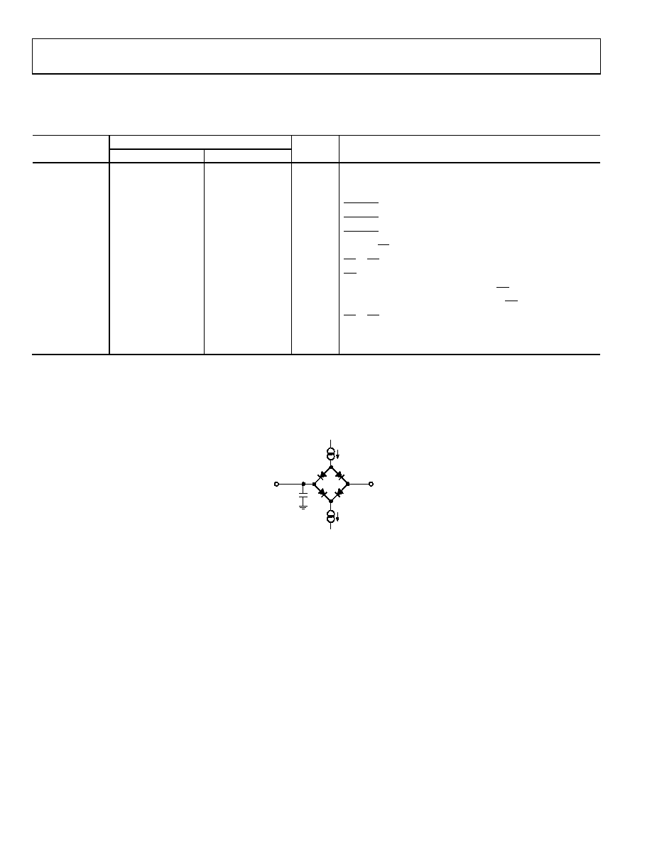
1.6V
200A
IOL
TO OUTPUT
PIN
CL
50pF
200A
IOH
0
11
28-
0
02
Figure 2. Load Circuit for Digital Output Timing Specifications
相关PDF资料 |
PDF描述 |
|---|---|
| ADM101EARMZ-REEL | IC TXRX RS-232 SINGLE 5V 10MSOP |
| VE-B1F-MY | CONVERTER MOD DC/DC 72V 50W |
| VE-B1D-MY | CONVERTER MOD DC/DC 85V 50W |
| VE-B1B-MY | CONVERTER MOD DC/DC 95V 50W |
| VE-B1B-MW | CONVERTER MOD DC/DC 95V 100W |
相关代理商/技术参数 |
参数描述 |
|---|---|
| AD7492BRU | 功能描述:IC ADC 12BIT W/REF W/CLK 24TSSOP RoHS:否 类别:集成电路 (IC) >> 数据采集 - 模数转换器 系列:- 产品培训模块:Lead (SnPb) Finish for COTS Obsolescence Mitigation Program 标准包装:2,500 系列:- 位数:12 采样率(每秒):3M 数据接口:- 转换器数目:- 功率耗散(最大):- 电压电源:- 工作温度:- 安装类型:表面贴装 封装/外壳:SOT-23-6 供应商设备封装:SOT-23-6 包装:带卷 (TR) 输入数目和类型:- |
| AD7492BRU-5 | 制造商:Analog Devices 功能描述:ADC Single SAR 1.25Msps 12-bit Parallel 24-Pin TSSOP 制造商:Rochester Electronics LLC 功能描述:1.5MSPS 12-BIT ADC, INTERNAL REF + CLOCK - Bulk |
| AD7492BRU-5-REEL | 制造商:Analog Devices 功能描述:ADC Single SAR 1.25Msps 12-bit Parallel 24-Pin TSSOP T/R 制造商:Analog Devices 功能描述:ADC SGL SAR 1.25MSPS 12-BIT PARALLEL 24TSSOP - Tape and Reel |
| AD7492BRU-5-REEL7 | 制造商:Analog Devices 功能描述:ADC Single SAR 1.25Msps 12-bit Parallel 24-Pin TSSOP T/R 制造商:Analog Devices 功能描述:ADC SGL SAR 1.25MSPS 12-BIT PARALLEL 24TSSOP - Tape and Reel |
| AD7492BRU-REEL | 功能描述:IC ADC 12BIT W/REF W/CLK 24TSSOP RoHS:否 类别:集成电路 (IC) >> 数据采集 - 模数转换器 系列:- 标准包装:1,000 系列:- 位数:12 采样率(每秒):300k 数据接口:并联 转换器数目:1 功率耗散(最大):75mW 电压电源:单电源 工作温度:0°C ~ 70°C 安装类型:表面贴装 封装/外壳:24-SOIC(0.295",7.50mm 宽) 供应商设备封装:24-SOIC 包装:带卷 (TR) 输入数目和类型:1 个单端,单极;1 个单端,双极 |
发布紧急采购,3分钟左右您将得到回复。