参数资料
| 型号: | AD7495BR |
| 厂商: | Analog Devices Inc |
| 文件页数: | 16/25页 |
| 文件大小: | 0K |
| 描述: | IC ADC 12BIT SRL LP W/REF 8-SOIC |
| 产品变化通告: | AD7495 Obsolescence 15/Apr/2011 |
| 标准包装: | 1 |
| 位数: | 12 |
| 采样率(每秒): | 1M |
| 数据接口: | DSP,MICROWIRE?,QSPI?,串行,SPI? |
| 转换器数目: | 1 |
| 功率耗散(最大): | 10.5mW |
| 电压电源: | 单电源 |
| 工作温度: | -40°C ~ 85°C |
| 安装类型: | 表面贴装 |
| 封装/外壳: | 8-SOIC(0.154",3.90mm 宽) |
| 供应商设备封装: | 8-SOIC |
| 包装: | 管件 |
| 输入数目和类型: | 1 个单端,单极 |
AD7475/AD7495
Rev. B | Page 22 of 24
The timer registers are loaded with a value that provides an
interrupt at the required sample interval. When an interrupt is
received, a value is transmitted with TFS/DT (ADC control
word). The TFS is used to control the RFS, and therefore, the
reading of data. The frequency of the serial clock is set in the
SCLKDIV register. When the instruction to transmit with TFS
is given, (that is, AX0 = TX0), the state of the SCLK is checked.
The DSP waits until the SCLK has gone high, low, and high
before transmission starts. If the timer and SCLK values are
chosen such that the instruction to transmit occurs on or near
the rising edge of SCLK, the data can be transmitted or it can
wait until the next clock edge.
For example, the ADSP-2111 has a master clock frequency of
16 MHz. If the SCLKDIV register is loaded with the value 3, an
SCLK of 2 MHz is obtained, and eight master clock periods
elapse for every one SCLK period. If the timer registers are
loaded with the value 803, 100.5 SCLKs occur between
interrupts and subsequently between transmit instructions.
This situation results in nonequidistant sampling because the
transmit instruction is occurring on a SCLK edge. If the
number of SCLKs between interrupts is a whole integer figure
of N, equidistant sampling is implemented by the DSP.
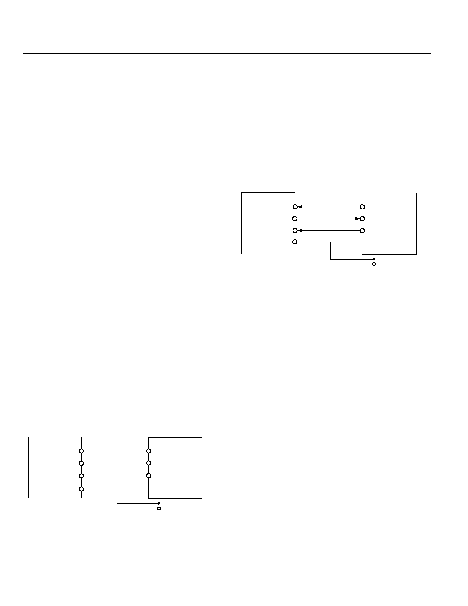
AD7475/AD7495 TO DSP56XXX
The connection diagram in Figure 30 shows how the AD7475/
AD7495 can be connected to the synchronous serial interface
(SSI) of the DSP56xxx family of devices from Motorola. The SSI
is operated in synchronous mode (SYN bit in CRB = 1) with
internally generated 1-bit clock period frame sync for both Tx
and Rx (Bits FSL1 = 1 and FSL0 = 0 in CRB). Set the word
length to 16 by setting Bits WL1 = 1 and WL0 = 0 in CRA. To
implement the power-down modes on the AD7475/AD7495,
the word length can be changed to 8 bits by setting Bit WL1 = 0
and Bit WL0 = 0 in CRA. For signal processing applications, it
is imperative that the frame synchronization signal from the
DSP56xxx provide equidistant sampling. The VDRIVE pin of the
AD7475/AD7495 takes the same supply voltage as that of the
DSP56xxx. This allows the ADC to operate at a voltage higher
than the serial interface, that is, DSP56xxx, if necessary.
AD7475/AD7495*
SCLK
*ADDITIONAL PINS OMITTED FOR CLARITY
SCLK
SC2
SDATA
VDRIVE
VDD
DSP56xxx*
SRD
01684-
B-
031
CS
Figure 30. Interfacing to the DSP56xxx
AD7475/AD7495 TO MC68HC16
The serial peripheral interface (SPI) on the MC68HC16 is
configured for master mode (MSTR) = 1, clock polarity bit
(CPOL) = 1, and the clock phase bit (CPHA) = 0. The SPI is
configured by writing to the SPI control register (SPCR), as
described in the 68HC16 User Manual. The serial transfer takes
place as a 16-bit operation when the size bit in the SPCR
register is set to size = 1. To implement the power-down modes
with an 8-bit transfer, set size = 0. (A connection diagram is
takes the same supply voltage as that of the MC68HC16. This
allows the ADC to operate at a higher voltage than the serial
interface, that is, the MC68HC16, if necessary.
AD7475/AD7495*
SCLK
*ADDITIONAL PINS OMITTED FOR CLARITY
MISO/PMC0
SS/PMC3
SDATA
VDRIVE
VDD
MC68HC16*
SCLK/PCM2
01684-
B-
032
CS
Figure 31. Interfacing to the MC68HC16
相关PDF资料 |
PDF描述 |
|---|---|
| V150B15M150BF3 | CONVERTER MOD DC/DC 15V 150W |
| AD7492BRU | IC ADC 12BIT W/REF W/CLK 24TSSOP |
| V150B15M150BF | CONVERTER MOD DC/DC 15V 150W |
| AD7475ARM-REEL7 | IC ADC 12BIT SRL LP 8-MSOP T/R |
| V150B15M150BL3 | CONVERTER MOD DC/DC 15V 150W |
相关代理商/技术参数 |
参数描述 |
|---|---|
| AD7495BRM | 功能描述:IC ADC 12BIT SRL LP W/REF 8MSOP RoHS:否 类别:集成电路 (IC) >> 数据采集 - 模数转换器 系列:- 产品培训模块:Lead (SnPb) Finish for COTS Obsolescence Mitigation Program 标准包装:2,500 系列:- 位数:12 采样率(每秒):3M 数据接口:- 转换器数目:- 功率耗散(最大):- 电压电源:- 工作温度:- 安装类型:表面贴装 封装/外壳:SOT-23-6 供应商设备封装:SOT-23-6 包装:带卷 (TR) 输入数目和类型:- |
| AD7495BRM-REEL | 功能描述:IC ADC 12BIT SRL LP W/REF 8MSOP RoHS:否 类别:集成电路 (IC) >> 数据采集 - 模数转换器 系列:- 标准包装:1,000 系列:- 位数:16 采样率(每秒):45k 数据接口:串行 转换器数目:2 功率耗散(最大):315mW 电压电源:模拟和数字 工作温度:0°C ~ 70°C 安装类型:表面贴装 封装/外壳:28-SOIC(0.295",7.50mm 宽) 供应商设备封装:28-SOIC W 包装:带卷 (TR) 输入数目和类型:2 个单端,单极 |
| AD7495BRM-REEL7 | 制造商:Analog Devices 功能描述:ADC Single SAR 1Msps 12-bit Serial 8-Pin MSOP T/R 制造商:Rochester Electronics LLC 功能描述:FAST 12-BIT LOW POWER SERIAL ADC I.C. - Tape and Reel |
| AD7495BRMZ | 功能描述:IC ADC 12BIT SRL LP W/REF 8MSOP RoHS:是 类别:集成电路 (IC) >> 数据采集 - 模数转换器 系列:- 其它有关文件:TSA1204 View All Specifications 标准包装:1 系列:- 位数:12 采样率(每秒):20M 数据接口:并联 转换器数目:2 功率耗散(最大):155mW 电压电源:模拟和数字 工作温度:-40°C ~ 85°C 安装类型:表面贴装 封装/外壳:48-TQFP 供应商设备封装:48-TQFP(7x7) 包装:Digi-Reel® 输入数目和类型:4 个单端,单极;2 个差分,单极 产品目录页面:1156 (CN2011-ZH PDF) 其它名称:497-5435-6 |
| AD7495BR-REEL | 功能描述:IC ADC 12BIT SRL LP W/REF 8-SOIC RoHS:否 类别:集成电路 (IC) >> 数据采集 - 模数转换器 系列:- 产品培训模块:Lead (SnPb) Finish for COTS Obsolescence Mitigation Program 标准包装:2,500 系列:- 位数:12 采样率(每秒):3M 数据接口:- 转换器数目:- 功率耗散(最大):- 电压电源:- 工作温度:- 安装类型:表面贴装 封装/外壳:SOT-23-6 供应商设备封装:SOT-23-6 包装:带卷 (TR) 输入数目和类型:- |
发布紧急采购,3分钟左右您将得到回复。