- 您现在的位置:买卖IC网 > PDF目录11477 > AD75019JPZ (Analog Devices Inc)IC CROSSPOINT SWIT 16X16 44PLCC PDF资料下载
参数资料
| 型号: | AD75019JPZ |
| 厂商: | Analog Devices Inc |
| 文件页数: | 2/4页 |
| 文件大小: | 0K |
| 描述: | IC CROSSPOINT SWIT 16X16 44PLCC |
| 标准包装: | 27 |
| 功能: | 交叉点开关 |
| 电路: | 1 x 16:16 |
| 导通状态电阻: | 300 欧姆 |
| 电压电源: | 单/双电源 |
| 电压 - 电源,单路/双路(±): | 4.5 V ~ 5.5 V,±12 V |
| 电流 - 电源: | 800µA |
| 工作温度: | -25°C ~ 85°C |
| 安装类型: | 表面贴装 |
| 封装/外壳: | 44-LCC(J 形引线) |
| 供应商设备封装: | 44-PLCC(16.59x16.59) |
| 包装: | 管件 |
REV. C
–2–
AD75019–SPECIFICATIONS1
AD75019
Symbol
Min
Typ
Max
Units
MULTIPLEXER
Input Signal Range
VIN
VSS – 0.5
VDD + 0.5
V
Switch ON Resistance, VDD and VSS = ± 12 V, VSIGNAL = ± 12 V
RON
150
300
Switch ON Resistance, VDD and VSS = ± 5 V, VSIGNAL = ± 5 V
RON
300
500
Switch ON Resistance Matching
2, V
SIGNAL = ± 12 V
R
ON
20
30
Leakage Current, VSIGNAL = ± 10 V
2
10
nA
Input/Output Capacitance
CIN
25
pF
Isolation Between Any Two Channels
RS = 600 , RL = 10 k, VSIGNAL = 2 V p-p
fSIGNAL = 1 kHz
92
dB
fSIGNAL = 20 kHz
69
dB
fSIGNAL = 1 MHz
38
dB
Total Harmonic Distortion
RS = 600 , RL = 10 k, VSIGNAL = 2 V p-p
0.01
%
Switch Frequency Response, –3 dB
RS = 600 , RL = 10 k, VSIGNAL = 2 V p-p
20
MHz
Propagation Delay
48
ns
DIGITAL INPUTS (SIN, SCLK, PCLK)
Logic Levels (TTL Compatible)
Input Voltage, Logic “1”
VIH
2.4
5.5
V
Input Voltage, Logic “0”
VIL
0
0.8
V
Input Current, VIH = 5.5 V
IIH
±1
A
Input Current, VIL = 0.8 V
IIL
±1
A
Input Capacitance
CIN
10
pF
DIGITAL OUTPUTS (SOUT)
Logic Levels (TTL Compatible)
Output Voltage, Logic “1”
VOH
2.8
V
Output Voltage, Logic “0”
VOL
0.4
V
Output Current, VOH = 2.8 V
IOH
3.2
mA
Output Current, VOL = 0.4 V
IOL
3.2
mA
POWER SUPPLY REQUIREMENTS
Voltage Range, Total Analog
VDD – VSS
9.0
25.2
V
Voltage Range, Positive Analog
VDD – VDGND
(VCC – 0.5)
25.2
V
Voltage Range, Negative Analog
VSS – VDGND
–20.7
0
V
Voltage Range, Digital
VCC – VDGND
4.5
5
5.5
V
Supply Current, SCLK = 5 MHz,
IDD, ISS
±70
mA
VIL = 0.8 V, VIH = 2.4 V
ICC
800
A
Supply Current, Quiescent,
IDD, ISS
_
400
A
VIL = 0.8 V, VIH = 2.4 V
ICC
_
100
A
TEMPERATURE RANGE
Operating
TMIN, TMAX
–25
+85
°C
Storage
–65
+150
°C
NOTES
1All minimum and maximum specifications are guaranteed, and specifications shown in boldface are tested on all production units at final electrical test. Results from those tests
are used to calculate outgoing quality levels.
2Switch resistance matching is measured with zero volts at each analog input and refers to the difference between the maximum and minimum values.
Specifications subject to change without notice.
(TA = +25 C, VDD and VSS =
12 V, VCC = +5 V unless otherwise noted)
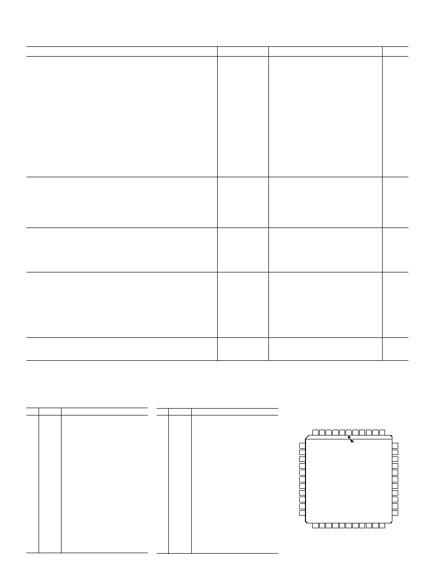
PIN CONFIGURATION
6
5
4
3
2
1
44 43 42 41 40
PIN 1
IDENTIFIER
TOP VIEW
(Not to Scale)
39
38
37
36
35
34
33
32
31
30
29
7
8
9
10
11
12
13
14
15
16
17
18 19 20 21 22 23 24 25 26 27 28
NC = NO CONNECT
NC
Y7
Y6
Y5
Y4
Y3
Y2
Y1
Y0
X15
X14
Y15
Y14
Y13
Y12
Y11
Y10
Y9
Y8
X0
X1
X2
NC
V
SS
SIN
SCLK
PCLK
SOUT
X3
X4
X5
X6
X8
X9
X10
X11
X12
X13
X7
DGND
V
CC
V
DD
NC
AD75019
PIN FUNCTION DESCRIPTIONS
Pin
Name
Description
1
PCLK
Parallel Clock Input
2
SCLK
Serial Clock Input
3
SIN
Serial Data Input
4VSS
Negative Analog Power Supply
5
NC
No Internal Connection
6
NC
No Internal Connection
7
Y15
Analog Output (or Input)
8
Y14
Analog Output (or Input)
9
Y13
Analog Output (or Input)
10
Y12
Analog Output (or Input)
11
Y11
Analog Output (or Input)
12
Y10
Analog Output (or Input)
13
Y9
Analog Output (or Input)
14
Y8
Analog Output (or Input)
15
X0
Analog Input (or Output)
16
X1
Analog Input (or Output)
17
X2
Analog Input (or Output)
18
X3
Analog Input (or Output)
19
X4
Analog Input (or Output)
20
X5
Analog Input (or Output)
21
X6
Analog Input (or Output)
22
X7
Analog Input (or Output)
Pin
Name
Description
23
X8
Analog Input (or Output)
24
X9
Analog Input (or Output)
25
X10
Analog Input (or Output)
26
X11
Analog Input (or Output)
27
X12
Analog Input (or Output)
28
X13
Analog Input (or Output)
29
X14
Analog Output (or Input)
30
X15
Analog Output (or Input)
31
Y0
Analog Output (or Input)
32
Y1
Analog Output (or Input)
33
Y2
Analog Output (or Input)
34
Y3
Analog Output (or Input)
35
Y4
Analog Output (or Input)
36
Y5
Analog Output (or Input)
37
Y6
Analog Output (or Input)
38
Y7
Analog Output (or Input)
39
NC
No Internal Connection
40
NC
No Internal Connection
41
VDD
Positive Analog Power Supply
42
VCC
Digital Power Supply
43
DGND Digital Ground
44
SOUT
Serial Data Output: Positive True
相关PDF资料 |
PDF描述 |
|---|---|
| SY58024UMG | IC CROSSPOINT SWITCH DUAL 32MLF |
| SY58040UMY | IC CROSSPOINT SWITCH 4X4 44MLF |
| PIC16F726-E/ML | IC PIC MCU FLASH 8KX14 28-QFN |
| PIC18LF2321T-I/ML | IC PIC MCU FLASH 4KX16 28QFN |
| PIC32MX130F064BT-V/SS | IC MCU 32BIT 64KB FLASH 28SSOP |
相关代理商/技术参数 |
参数描述 |
|---|---|
| AD75019JPZ-REEL | 制造商:Analog Devices 功能描述:ANLG GEN PURPOSE CROSSPOINT 16 X 16 44PLCC - Tape and Reel |
| AD7501JD | 制造商:AD 制造商全称:Analog Devices 功能描述:4 / 8 Channel Analog Multiplexers |
| AD7501JN | 功能描述:IC MULTIPLEXER 8X1 16DIP RoHS:否 类别:集成电路 (IC) >> 接口 - 模拟开关,多路复用器,多路分解器 系列:- 其它有关文件:STG4159 View All Specifications 标准包装:5,000 系列:- 功能:开关 电路:1 x SPDT 导通状态电阻:300 毫欧 电压电源:双电源 电压 - 电源,单路/双路(±):±1.65 V ~ 4.8 V 电流 - 电源:50nA 工作温度:-40°C ~ 85°C 安装类型:表面贴装 封装/外壳:7-WFBGA,FCBGA 供应商设备封装:7-覆晶 包装:带卷 (TR) |
| AD7501JNZ | 功能描述:IC MULTIPLEXER 8X1 16DIP RoHS:是 类别:集成电路 (IC) >> 接口 - 模拟开关,多路复用器,多路分解器 系列:- 应用说明:Ultrasound Imaging Systems Application Note 产品培训模块:Lead (SnPb) Finish for COTS Obsolescence Mitigation Program 标准包装:250 系列:- 功能:开关 电路:单刀单掷 导通状态电阻:48 欧姆 电压电源:单电源 电压 - 电源,单路/双路(±):2.7 V ~ 5.5 V 电流 - 电源:5µA 工作温度:0°C ~ 70°C 安装类型:表面贴装 封装/外壳:48-LQFP 供应商设备封装:48-LQFP(7x7) 包装:托盘 |
| AD7501JP | 制造商:未知厂家 制造商全称:未知厂家 功能描述:8-Channel Analog Multiplexer |
发布紧急采购,3分钟左右您将得到回复。