参数资料
| 型号: | AD7524KNZ |
| 厂商: | Analog Devices Inc |
| 文件页数: | 4/8页 |
| 文件大小: | 0K |
| 描述: | IC DAC 8BIT MULTIPLYING 16-DIP |
| 产品培训模块: | Data Converter Fundamentals DAC Architectures |
| 标准包装: | 25 |
| 设置时间: | 250ns |
| 位数: | 8 |
| 数据接口: | 并联 |
| 转换器数目: | 1 |
| 电压电源: | 单电源 |
| 功率耗散(最大): | 30mW |
| 工作温度: | -40°C ~ 85°C |
| 安装类型: | 通孔 |
| 封装/外壳: | 16-DIP(0.300",7.62mm) |
| 供应商设备封装: | 16-PDIP |
| 包装: | 管件 |
| 输出数目和类型: | 2 电流,单极;2 电流,双极 |
| 采样率(每秒): | 4M |
| 产品目录页面: | 784 (CN2011-ZH PDF) |
AD7524
REV. B
–4–
WRITE MODE
When CS and WR are both LOW, the AD7524 is in the
WRITE mode, and the AD7524 analog output responds to data
activity at the DB0–DB7 data bus inputs. In this mode, the
AD7524 acts like a nonlatched input D/A converter.
HOLD MODE
When either CS or WR is HIGH, the AD7524 is in the HOLD
mode. The AD7524 analog output holds the value correspond-
ing to the last digital input present at DB0–DB7 prior to WR or
CS
assuming the HIGH state.
MODE SELECTION TABLE
CS
WR
Mode
DAC Response
L
Write
DAC responds to data bus
(DB0–DB7) inputs.
H
X
Hold
Data bus (DB0–DB7) is
Locked Out:
X
H
Hold
DAC holds last data present
when WR or CS assumed
HIGH state.
L = Low State, H = High State, X = Don't Care.
WRITE CYCLE TIMING DIAGRAM
Figure 3. Supply Current vs. Logic Level
Typical plots of supply current, IDD, versus logic input voltage,
VIN, for VDD = +5 V and VDD = +15 V are shown above.
CIRCUIT DESCRIPTION
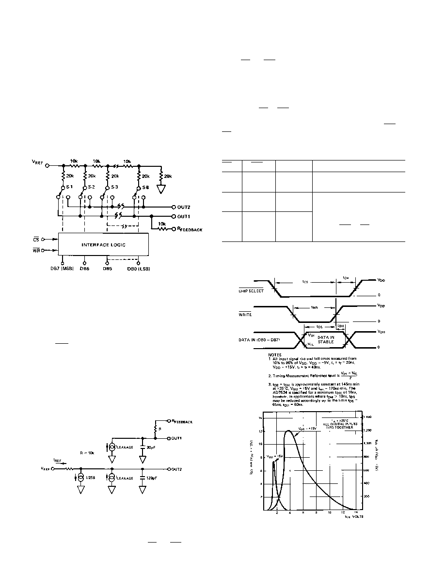
CIRCUIT INFORMATION
The AD7524, an 8-bit multiplying D/A converter, consists of a
highly stable thin film R-2R ladder and eight N-channel current
switches on a monolithic chip. Most applications require the
addition of only an output operational amplifier and a voltage
or current reference.
The simplified D/A circuit is shown in Figure 1. An inverted
R-2R ladder structure is used—that is, the binarily weighted
currents are switched between the OUT1 and OUT2 bus lines,
thus maintaining a constant current in each ladder leg indepen-
dent of the switch state.
Figure 1. Functional Diagram
EQUIVALENT CIRCUIT ANALYSIS
The equivalent circuit for all digital inputs LOW is shown in
Figures 2. In Figure 2 with all digital inputs LOW, the refer-
ence current is switched to OUT2. The current source ILEAKAGE
is composed of surface and junction leakages to the substrate
while the
1
256
current source represents a constant 1-bit cur-
rent drain through the termination resistor on the R-2R ladder.
The “ON” capacitance of the output N-channel switches is
120 pF, as shown on the OUT2 terminal. The “OFF” switch
capacitance is 30 pF, as shown on the OUT1 terminal. Analysis
of the circuit for all digital inputs high is similar to Figure 2
however, the “ON” switches are now on terminal OUT1, hence
the 120 pF appears at that terminal.
Figure 2. AD7524 DAC Equivalent Circuit—All Digital
Inputs Low
INTERFACE LOGIC INFORMATION
MODE SELECTION
AD7524 mode selection is controlled by the CS and WR inputs.
相关PDF资料 |
PDF描述 |
|---|---|
| MS3454W22-14PW | CONN RCPT 19POS JAM NUT W/PINS |
| AD8804ANZ | IC DAC 8BIT 12CH W/SD 20DIP |
| VE-B1J-MV-F3 | CONVERTER MOD DC/DC 36V 150W |
| MS3454W22-14P | CONN RCPT 19POS JAM NUT W/PINS |
| AD5335BRUZ | IC DAC 10BIT QUAD VOUT 24TSSOP |
相关代理商/技术参数 |
参数描述 |
|---|---|
| AD7524KP | 功能描述:IC DAC 8BIT MULTIPLYING 20-PLCC RoHS:否 类别:集成电路 (IC) >> 数据采集 - 数模转换器 系列:- 标准包装:2,400 系列:- 设置时间:- 位数:18 数据接口:串行 转换器数目:3 电压电源:模拟和数字 功率耗散(最大):- 工作温度:-40°C ~ 85°C 安装类型:表面贴装 封装/外壳:36-TFBGA 供应商设备封装:36-TFBGA 包装:带卷 (TR) 输出数目和类型:* 采样率(每秒):* |
| AD7524KP-REEL | 制造商:Rochester Electronics LLC 功能描述:- Tape and Reel |
| AD7524KPZ | 制造商:Analog Devices 功能描述:DAC 1-CH R-2R 8-bit 20-Pin PLCC 制造商:Analog Devices 功能描述:DAC 1-Ch R-2R 8-Bit 20-Pin PLCC |
| AD7524KPZ-REEL | 功能描述:8 Bit Digital to Analog Converter 1 20-PLCC (9x9) 制造商:analog devices inc. 系列:- 包装:带卷(TR) 零件状态:初步 位数:8 数模转换器数:1 建立时间:500ns 输出类型:Current - Buffered 差分输出:是 数据接口:并联 参考类型:外部 电压 - 电源,模拟:5 V ~ 15 V 电压 - 电源,数字:5 V ~ 15 V INL/DNL(LSB):±0.5(最大),- 架构:R-2R 工作温度:-40°C ~ 85°C 封装/外壳:20-LCC(J 形引线) 供应商器件封装:20-PLCC(9x9) 标准包装:1,000 |
| AD7524LB | 功能描述:鼓风机 75mm 24VDC 6.9CFM RoHS:否 制造商:Murata 产品:Blowers 电流类型:DC 电源电压:5.3 V 气流:1 l/min 轴承类型: 噪声: 速度: 功率额定值: 框架尺寸 (mm):20 mm x 20 mm x 1.85 mm 外壳材料: 端接类型:SMD/SMT 系列:MZB |
发布紧急采购,3分钟左右您将得到回复。