参数资料
| 型号: | AD7528JP |
| 厂商: | Analog Devices Inc |
| 文件页数: | 6/8页 |
| 文件大小: | 0K |
| 描述: | IC DAC 8BIT DUAL MULT 20-PLCC |
| 产品培训模块: | Data Converter Fundamentals DAC Architectures |
| 标准包装: | 49 |
| 设置时间: | 400ns |
| 位数: | 8 |
| 数据接口: | 并联 |
| 转换器数目: | 2 |
| 电压电源: | 单电源 |
| 功率耗散(最大): | 450mW |
| 工作温度: | -40°C ~ 85°C |
| 安装类型: | 表面贴装 |
| 封装/外壳: | 20-LCC(J 形引线) |
| 供应商设备封装: | 20-PLCC(9x9) |
| 包装: | 管件 |
| 输出数目和类型: | 2 电流,单极;2 电流,双极 |
AD7528
REV. B
–6–
APPLICATIONS INFORMATION
Application Hints
To ensure system performance consistent with AD7528 specifi-
cations, careful attention must be given to the following points:
1. GENERAL GROUND MANAGEMENT: AC or transient
voltages between the AD7528 AGND and DGND can cause
noise injection into the analog output. The simplest method
of ensuring that voltages at AGND and DGND are equal is
to tie AGND and DGND together at the AD7528. In more
complex systems where the AGND–DGND intertie is on the
backplane, it is recommended that diodes be connected in
inverse parallel between the AD7528 AGND and DGND
pins (1N914 or equivalent).
2. OUTPUT AMPLIFIER OFFSET: CMOS DACs exhibit a
code-dependent output resistance which in turn causes a
code-dependent amplifier noise gain. The effect is a code-
dependent differential nonlinearity term at the amplifier
output which depends on VOS (VOS is amplifier input offset
voltage). This differential nonlinearity term adds to the R/2R
differential nonlinearity. To maintain monotonic operation, it
is recommended that amplifier VOS be no greater than 10% of
1 LSB over the temperature range of interest.
3. HIGH FREQUENCY CONSIDERATIONS: The output
capacitance of a CMOS DAC works in conjunction with the
amplifier feedback resistance to add a pole to the open loop
response. This can cause ringing or oscillation. Stability can
be restored by adding a phase compensation capacitor in
parallel with the feedback resistor.
DYNAMIC PERFORMANCE
The dynamic performance of the two DACs in the AD7528 will
depend upon the gain and phase characteristics of the output
amplifiers together with the optimum choice of the PC board
layout and decoupling components. Figure 6 shows the relation
INPUT FREQUENCY – Hz
–100
ISOLATION
–
dB
20k
50k
100k
200k
1M
500k
–90
–80
–70
–60
–50
TA = +25 C
VDD = +15V
VIN = 20V PEAK TO PEAK
Figure 6. Channel-to-Channel Isolation
AGND
V+
V–
AD644
VREF B*
VDD
CS
LSB
C1 LOCATION
C2 LOCATION
VREF A*
DGND
DAC A/DAC B
MSB
PIN 8 OF TO-5 CAN (AD644)
AD7528 PIN 1
WR
AD7528
*NOTE
INPUT SCREENS
TO REDUCE
FEEDTHROUGH.
LAYOUT SHOWS
COPPER SIDE
(i.e., BOTTOM VIEW).
Figure 7. Suggested PC Board Layout for AD7528 with
AD644 Dual Op Amp
ship between input frequency and channel to channel isolation.
Figure 7 shows a printed circuit layout for the AD7528 and the
AD644 dual op amp which minimizes feedthrough and crosstalk.
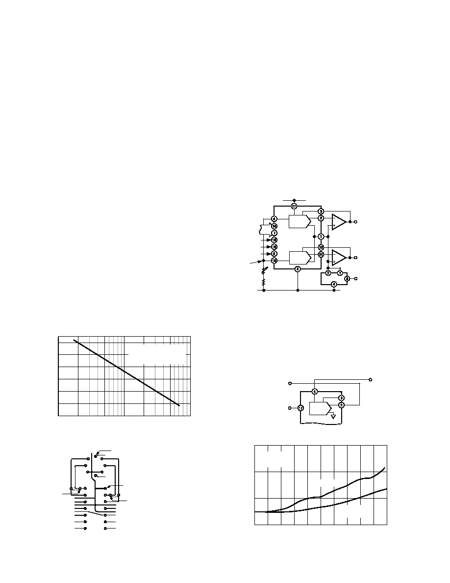
SINGLE SUPPLY APPLICATIONS
The AD7528 DAC R-2R ladder termination resistors are con-
nected to AGND within the device. This arrangement is par-
ticularly convenient for single supply operation because AGND
may be biased at any voltage between DGND and VDD. Figure
8 shows a circuit which provides two +5 V to +8 V analog out-
puts by biasing AGND +5 V up from DGND. The two DAC
reference inputs are tied together and a reference input voltage
is obtained without a buffer amplifier by making use of the
constant and matched impedances of the DAC A and DAC B
reference inputs. Current flows through the two DAC R-2R
ladders into R1 and R1 is adjusted until the VREF A and VREF B
inputs are at +2 V. The two analog output voltages range from
+5 V to +8 V for DAC codes 00000000 to 11111111.
VOUT A = +5V TO +8V
VDD
DATA
INPUTS
DAC A/DAC B
CS
WR
GND
VDD = +15V
SUGGESTED
OP AMP:
AD644
VOUT B = +5V TO +8V
R1
10k
2 VOLTS
R2
1k
AD584J
AD7528
DB0
DB7
DAC A
DAC B
Figure 8. AD7528 Single Supply Operation
Figure 9 shows DAC A of the AD7528 connected in a positive
reference, voltage switching mode. This configuration is useful
in that VOUT is the same polarity as VIN allowing single supply
operation. However, to retain specified linearity, VIN must be in
the range 0 V to +2.5 V and the output buffered or loaded with
a high impedance, see Figure 10. Note that the input voltage is
connected to the DAC OUT A and the output voltage is taken
from the DAC VREF A pin.
VREF A
VIN (0V TO +2.5V)
VDD
+15V
AD7528
DAC A
OUT A
VOUT
Figure 9. AD7528 in Single Supply, Voltage Switching Mode
VINA – Volts
3
2.5
ERROR
–
LSB
3.5
3456
7
2
1
TA = +25 C
VDD = +15V
4.5
5.5
6.5
7.5
NONLINEARITY
DIFFERENTIAL
NONLINEARITY
Figure 10. Typical AD7528 Performance in Single Supply
Voltage Switching Mode (K/B/T, L/C/U Grades)
相关PDF资料 |
PDF描述 |
|---|---|
| VI-243-MW-B1 | CONVERTER MOD DC/DC 24V 100W |
| VI-241-MW-B1 | CONVERTER MOD DC/DC 12V 100W |
| AD5546CRUZ-REEL7 | IC DAC 16BIT PAR 28TSSOP |
| VE-BTM-MV-B1 | CONVERTER MOD DC/DC 10V 150W |
| VI-25M-IV-F4 | CONVERTER MOD DC/DC 10V 150W |
相关代理商/技术参数 |
参数描述 |
|---|---|
| AD7528JP-REEL | 功能描述:IC DAC 8BIT DUAL MULT 20-PLCC RoHS:否 类别:集成电路 (IC) >> 数据采集 - 数模转换器 系列:- 标准包装:47 系列:- 设置时间:2µs 位数:14 数据接口:并联 转换器数目:1 电压电源:单电源 功率耗散(最大):55µW 工作温度:-40°C ~ 85°C 安装类型:表面贴装 封装/外壳:28-SSOP(0.209",5.30mm 宽) 供应商设备封装:28-SSOP 包装:管件 输出数目和类型:1 电流,单极;1 电流,双极 采样率(每秒):* |
| AD7528JPZ | 功能描述:IC DAC 8BIT DUAL MULT 20PLCC RoHS:是 类别:集成电路 (IC) >> 数据采集 - 数模转换器 系列:- 标准包装:1 系列:- 设置时间:4.5µs 位数:12 数据接口:串行,SPI? 转换器数目:1 电压电源:单电源 功率耗散(最大):- 工作温度:-40°C ~ 125°C 安装类型:表面贴装 封装/外壳:8-SOIC(0.154",3.90mm 宽) 供应商设备封装:8-SOICN 包装:剪切带 (CT) 输出数目和类型:1 电压,单极;1 电压,双极 采样率(每秒):* 其它名称:MCP4921T-E/SNCTMCP4921T-E/SNRCTMCP4921T-E/SNRCT-ND |
| AD7528JPZ-REEL | 功能描述:IC DAC 8BIT DUAL MULT 20PLCC RoHS:是 类别:集成电路 (IC) >> 数据采集 - 数模转换器 系列:- 标准包装:47 系列:- 设置时间:2µs 位数:14 数据接口:并联 转换器数目:1 电压电源:单电源 功率耗散(最大):55µW 工作温度:-40°C ~ 85°C 安装类型:表面贴装 封装/外壳:28-SSOP(0.209",5.30mm 宽) 供应商设备封装:28-SSOP 包装:管件 输出数目和类型:1 电流,单极;1 电流,双极 采样率(每秒):* |
| AD7528JR | 功能描述:IC DAC 8BIT DUAL MULTIPLY 20SOIC RoHS:否 类别:集成电路 (IC) >> 数据采集 - 数模转换器 系列:- 产品培训模块:Data Converter Fundamentals DAC Architectures 标准包装:750 系列:- 设置时间:7µs 位数:16 数据接口:并联 转换器数目:1 电压电源:双 ± 功率耗散(最大):100mW 工作温度:0°C ~ 70°C 安装类型:表面贴装 封装/外壳:28-LCC(J 形引线) 供应商设备封装:28-PLCC(11.51x11.51) 包装:带卷 (TR) 输出数目和类型:1 电压,单极;1 电压,双极 采样率(每秒):143k |
| AD7528JR-REEL | 功能描述:IC DAC 8BIT DUAL MULT 20-SOIC RoHS:否 类别:集成电路 (IC) >> 数据采集 - 数模转换器 系列:- 标准包装:2,400 系列:- 设置时间:- 位数:18 数据接口:串行 转换器数目:3 电压电源:模拟和数字 功率耗散(最大):- 工作温度:-40°C ~ 85°C 安装类型:表面贴装 封装/外壳:36-TFBGA 供应商设备封装:36-TFBGA 包装:带卷 (TR) 输出数目和类型:* 采样率(每秒):* |
发布紧急采购,3分钟左右您将得到回复。