参数资料
| 型号: | AD7528JR |
| 厂商: | Analog Devices Inc |
| 文件页数: | 3/8页 |
| 文件大小: | 0K |
| 描述: | IC DAC 8BIT DUAL MULTIPLY 20SOIC |
| 产品培训模块: | Data Converter Fundamentals DAC Architectures |
| 标准包装: | 37 |
| 设置时间: | 400ns |
| 位数: | 8 |
| 数据接口: | 并联 |
| 转换器数目: | 2 |
| 电压电源: | 单电源 |
| 功率耗散(最大): | 450mW |
| 工作温度: | -40°C ~ 85°C |
| 安装类型: | 表面贴装 |
| 封装/外壳: | 20-SOIC(0.295",7.50mm 宽) |
| 供应商设备封装: | 20-SOIC W |
| 包装: | 管件 |
| 输出数目和类型: | 2 电流,单极;2 电流,双极 |
PLCC
3
2
1
20
19
9
10
11
12
13
18
17
16
15
14
4
5
6
7
8
TOP VIEW
(Not to Scale)
PIN 1
IDENTIFIER
VREF A
DGND
DAC A/DAC B
(MSB) DB7
DB6
VREF B
VDD
WR
CS
DB0 (LSB)
AD7528
R
FB
A
OUT
A
AGND
OUT
B
R
FB
B
DB5
DB4
DB3
DB2
DB1
VDD = +5 V
VDD = +15 V
Parameter
Version
1
TA = +25
°CT
MIN, TMAX
TA= +25
°CT
MIN, TMAX
Units
Test Conditions/Comments
CHANNEL-TO-CHANNEL ISOLATION
Both DAC Latches Loaded with 11111111.
VREF A to OUT B
All
–77
dB typ
VREF A = 20 V p-p Sine Wave @ 100 kHz
VREF B = 0 V see Figure 6.
VREF B to OUT A
–77
dB typ
VREF A = 20 V p-p Sine Wave @ 100 kHz
VREF A = 0 V see Figure 6.
DIGITAL CROSSTALK
All
30
60
nV sec typ
Measured for Code Transition 00000000 to
11111111
HARMONIC DISTORTlON
All
–85
dB typ
VIN = 6 V rms @ 1 kHz
NOTES
1Temperature Ranges are J, K, L Versions: –40
°C to +85°C
A, B, C Versions: –40
°C to +85°C
S, T, U Versions: –55
°C to +125°C
2Specifications applies to both DACs in AD7528.
3Guaranteed by design but not production tested.
4Logic inputs are MOS Gates. Typical input current (+25
°C) is less than 1 nA.
5These characteristics are for design guidance only and are not subject to test.
6Feedthrough can be further reduced by connecting the metal lid on the ceramic package
(suffix D) to DGND.
Specifications subject to change without notice.
AD7528, ideal maximum output is VREF – 1 LSB. Gain error of
both DACs is adjustable to zero with external resistance.
Output Capacitance
Capacitance from OUT A or OUT B to AGND.
Digital to Analog Glitch lmpulse
The amount of charge injected from the digital inputs to the
analog output when the inputs change state. This is normally
specified as the area of the glitch in either pA-secs or nV-secs
depending upon whether the glitch is measured as a current or
voltage signal. Glitch impulse is measured with VREF A,
VREF B = AGND.
Propagation Delay
This is a measure of the internal delays of the circuit and is
defined as the time from a digital input change to the analog
output current reaching 90% of its final value.
Channel-to-Channel Isolation
The proportion of input signal from one DAC’s reference input
which appears at the output of the other DAC, expressed as a
ratio in dB.
Digital Crosstalk
The glitch energy transferred to the output of one converter due
to a change in digital input code to the other converter. Speci-
fied in nV secs.
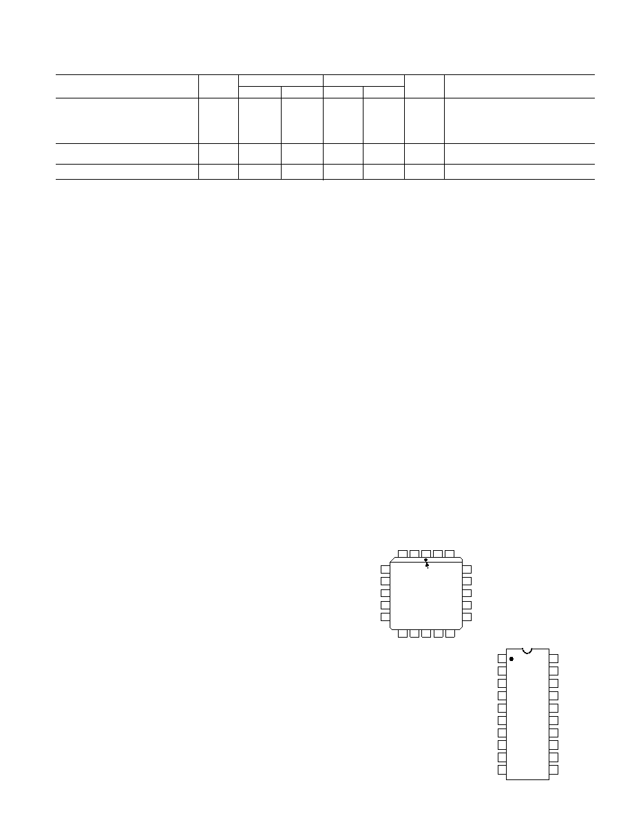
PIN CONFIGURATIONS
ABSOLUTE MAXIMUM RATINGS
(TA = +25
°C unless otherwise noted)
VDD to AGND . . . . . . . . . . . . . . . . . . . . . . . . . . . . 0 V, +17 V
VDD to DGND . . . . . . . . . . . . . . . . . . . . . . . . . . . . 0 V, +17 V
AGND to DGND . . . . . . . . . . . . . . . . . . . . . . . . VDD + 0.3 V
DGND to AGND . . . . . . . . . . . . . . . . . . . . . . . . VDD + 0.3 V
Digital Input Voltage to DGND . . . . . . . –0.3 V, VDD + 0.3 V
VPIN2, VPIN20 to AGND . . . . . . . . . . . . . . –0.3 V, VDD + 0.3 V
VREF A, VREF B to AGND . . . . . . . . . . . . . . . . . . . . . . .
±25 V
VRFB A, VRFB B to AGND . . . . . . . . . . . . . . . . . . . . . . .
±25 V
Power Dissipation (Any Package) to +75
°C . . . . . . . 450 mW
Derates above +75
°C by . . . . . . . . . . . . . . . . . . . 6 mW/°C
Operating Temperature Range
Commercial (J, K, L) Grades . . . . . . . . . . . –40
°C to +85°C
Industrial (A, B, C) Grades . . . . . . . . . . . . –40
°C to +85°C
Extended (S, T, U) Grades . . . . . . . . . . . –55
°C to +125°C
Storage Temperature . . . . . . . . . . . . . . . . . . –65
°C to +150°C
Lead Temperature (Soldering, 10 secs) . . . . . . . . . . . . +300
°C
CAUTION:
1. ESD sensitive device. The digital control inputs are diode
protected; however, permanent damage may occur on uncon-
nected devices subjected to high energy electrostatic fields.
Unused devices must be stored in conductive foam or shunts.
2. Do not insert this device into powered sockets. Remove
power before insertion or removal.
TERMINOLOGY
Relative Accuracy
Relative accuracy or endpoint nonlinearity is a measure of the
maximum deviation from a straight line passing through the
endpoints of the DAC transfer function. It is measured after
adjusting for zero and full scale and is normally expressed in
LSBs or as a percentage of full scale reading.
Differential Nonlinearity
Differential nonlinearity is the difference between the measured
change and the ideal 1 LSB change between any two adjacent
codes. A specified differential nonlinearity of
±1 LSB max over
the operating temperature range ensures monotonicity.
Gain Error
Gain error or full-scale error is a measure of the output error
between an ideal DAC and the actual device output. For the
AD7528
REV. B
–3–
DIP, SOIC
TOP VIEW
(Not to Scale)
20
19
18
17
16
15
14
13
12
11
1
2
3
4
5
6
7
8
9
10
AD7528
DB4
DB5
DB6
OUT A
RFB A
VREF A
(MSB) DB7
DAC A/DAC B
DGND
DB3
DB2
DB1
RFB B
VREF B
VDD
DB0 (LSB)
CS
WR
AGND
OUT B
相关PDF资料 |
PDF描述 |
|---|---|
| SY88923AVKG | IC POST AMP HS LIMITING 10-MSOP |
| LTC6400IUD-26#PBF | IC ADC DRIVER DIFF 16-QFN |
| SY88813VKG | IC AMP POST PECL 3.3V/5V 10-MSOP |
| LTC1591-1IG | IC D/A CONV 14BIT PAR 28-SSOP |
| LTC6406CUD#PBF | IC DIFF AMP/DRIVER R-R 16-QFN |
相关代理商/技术参数 |
参数描述 |
|---|---|
| AD7528JR-REEL | 功能描述:IC DAC 8BIT DUAL MULT 20-SOIC RoHS:否 类别:集成电路 (IC) >> 数据采集 - 数模转换器 系列:- 标准包装:2,400 系列:- 设置时间:- 位数:18 数据接口:串行 转换器数目:3 电压电源:模拟和数字 功率耗散(最大):- 工作温度:-40°C ~ 85°C 安装类型:表面贴装 封装/外壳:36-TFBGA 供应商设备封装:36-TFBGA 包装:带卷 (TR) 输出数目和类型:* 采样率(每秒):* |
| AD7528JR-REEL7 | 功能描述:IC DAC 8BIT DUAL MULT 20-SOIC RoHS:否 类别:集成电路 (IC) >> 数据采集 - 数模转换器 系列:- 标准包装:47 系列:- 设置时间:2µs 位数:14 数据接口:并联 转换器数目:1 电压电源:单电源 功率耗散(最大):55µW 工作温度:-40°C ~ 85°C 安装类型:表面贴装 封装/外壳:28-SSOP(0.209",5.30mm 宽) 供应商设备封装:28-SSOP 包装:管件 输出数目和类型:1 电流,单极;1 电流,双极 采样率(每秒):* |
| AD7528JRZ | 功能描述:IC DAC 8BIT DUAL MULT 20-SOIC RoHS:是 类别:集成电路 (IC) >> 数据采集 - 数模转换器 系列:- 产品培训模块:Lead (SnPb) Finish for COTS Obsolescence Mitigation Program 标准包装:50 系列:- 设置时间:4µs 位数:12 数据接口:串行 转换器数目:2 电压电源:单电源 功率耗散(最大):- 工作温度:-40°C ~ 85°C 安装类型:表面贴装 封装/外壳:8-TSSOP,8-MSOP(0.118",3.00mm 宽) 供应商设备封装:8-uMAX 包装:管件 输出数目和类型:2 电压,单极 采样率(每秒):* 产品目录页面:1398 (CN2011-ZH PDF) |
| AD7528JRZ-REEL | 功能描述:IC DAC 8BIT DUAL MULT 20-SOIC RoHS:是 类别:集成电路 (IC) >> 数据采集 - 数模转换器 系列:- 标准包装:47 系列:- 设置时间:2µs 位数:14 数据接口:并联 转换器数目:1 电压电源:单电源 功率耗散(最大):55µW 工作温度:-40°C ~ 85°C 安装类型:表面贴装 封装/外壳:28-SSOP(0.209",5.30mm 宽) 供应商设备封装:28-SSOP 包装:管件 输出数目和类型:1 电流,单极;1 电流,双极 采样率(每秒):* |
| AD7528JRZ-REEL7 | 功能描述:IC DAC 8BIT DUAL MULT 20SOIC RoHS:是 类别:集成电路 (IC) >> 数据采集 - 数模转换器 系列:- 产品培训模块:Lead (SnPb) Finish for COTS Obsolescence Mitigation Program 标准包装:50 系列:- 设置时间:4µs 位数:12 数据接口:串行 转换器数目:2 电压电源:单电源 功率耗散(最大):- 工作温度:-40°C ~ 85°C 安装类型:表面贴装 封装/外壳:8-TSSOP,8-MSOP(0.118",3.00mm 宽) 供应商设备封装:8-uMAX 包装:管件 输出数目和类型:2 电压,单极 采样率(每秒):* 产品目录页面:1398 (CN2011-ZH PDF) |
发布紧急采购,3分钟左右您将得到回复。