参数资料
| 型号: | AD7528KPZ-REEL |
| 厂商: | Analog Devices Inc |
| 文件页数: | 4/8页 |
| 文件大小: | 0K |
| 描述: | IC DAC 8BIT DUAL MULT 20PLCC |
| 产品培训模块: | Data Converter Fundamentals DAC Architectures |
| 标准包装: | 1,000 |
| 设置时间: | 400ns |
| 位数: | 8 |
| 数据接口: | 并联 |
| 转换器数目: | 2 |
| 电压电源: | 单电源 |
| 功率耗散(最大): | 450mW |
| 工作温度: | -40°C ~ 85°C |
| 安装类型: | 表面贴装 |
| 封装/外壳: | 20-LCC(J 形引线) |
| 供应商设备封装: | 20-PLCC(9x9) |
| 包装: | 带卷 (TR) |
| 输出数目和类型: | 2 电流,单极;2 电流,双极 |
AD7528
REV. B
–4–
INTERFACE LOGIC INFORMATION
DAC Selection:
Both DAC latches share a common 8-bit input port. The con-
trol input
DAC A/DAC B selects which DAC can accept data
from the input port.
Mode Selection:
Inputs
CS and WR control the operating mode of the selected
DAC. See Mode Selection Table below.
Write Mode:
When
CS and WR are both low the selected DAC is in the write
mode. The input data latches of the selected DAC are transpar-
ent and its analog output responds to activity on DB0–DB7.
Hold Mode:
The selected DAC latch retains the data which was present on
DB0–DB7 just prior to
CS or WR assuming a high state. Both
analog outputs remain at the values corresponding to the data in
their respective latches.
Mode Selection Table
DAC A/DAC B
CS
WR
DAC A
DAC B
L
WRITE
HOLD
H
L
HOLD
WRITE
X
H
X
HOLD
X
H
HOLD
L = Low State; H = High State; X = Don’t Care.
WRITE CYCLE TIMING DIAGRAM
VDD
tDH
VIH
VIL
tDS
tWR
tAS
tAH
tCS
tCH
VDD
0
CHIP SELECT
DAC A/DAC B
WRITE
DATA IN
(DB0 – DB7)
DATA IN STABLE
NOTES:
1. ALL INPUT SIGNAL RISE AND FALL TIMES MEASURED
FROM 10% TO 90% OF VDD.
VDD = +5V, tr = tf = 20ns;
VDD = +15V, tr = tf = 40ns;
2. TIMING MEASUREMENT REFERENCE LEVEL IS
VIH + VIL
2
CIRCUIT INFORMATION—D/A SECTION
The AD7528 contains two identical 8-bit multiplying D/A con-
verters, DAC A and DAC B. Each DAC consists of a highly
stable thin film R-2R ladder and eight N-channel current steer-
ing switches. A simplified D/A circuit for DAC A is shown in
VREF A
AGND
DAC A DATA LATCHES
AND DRIVERS
2R
S1
2R
S2
2R
S3
2R
S8
2R
R
OUT A
RFB A
R
Figure 1. Simplified Functional Circuit for DAC A
Figure 1. An inverted R-2R ladder structure is used, that is, bi-
nary weighted currents are switched between the DAC output
and AGND thus maintaining fixed currents in each ladder leg
independent of switch state.
EQUIVALENT CIRCUIT ANALYSIS
Figure 2 shows an approximate equivalent circuit for one of the
AD7528’s D/A converters, in this case DAC A. A similar
equivalent circuit can be drawn for DAC B. Note that AGND
(Pin 1) is common for both DAC A and DAC B.
The current source ILEAKAGE is composed of surface and junc-
tion leakages and, as with most semiconductor devices, approxi-
mately doubles every 10
°C. The resistor R
O as shown in Figure
2 is the equivalent output resistance of the device which varies
with input code (excluding all 0s code) from 0.8 R to 2 R. R is
typically 11 k
. C
OUT is the capacitance due to the N-channel
switches and varies from about 50 pF to 120 pF depending
upon the digital input. g(VREF A, N) is the Thevenin equivalent
voltage generator due to the reference input voltage VREF A and
the transfer function of the R-2R ladder.
RFB A
AGND
OUT A
RO
g(VREF A, N)
ILKG
COUT
R
Figure 2. Equivalent Analog Output Circuit of DAC A
CIRCUIT INFORMATION–DIGITAL SECTION
The input buffers are simple CMOS inverters designed such
that when the AD7528 is operated with VDD = 5 V, the buffer
converts TTL input levels (2.4 V and 0.8 V) into CMOS logic
levels. When VIN is in the region of 2.0 volts to 3.5 volts the
input buffers operate in their linear region and pass a quiescent
current, see Figure 3. To minimize power supply currents it is
recommended that the digital input voltages be as close to the
supply rails (VDD and DGND) as is practically possible.
The AD7528 may be operated with any supply voltage in the
range 5
≤ V
DD
≤ 15 volts. With V
DD = +15 V the input logic
levels are CMOS compatible only, i.e., 1.5 V and 13.5 V.
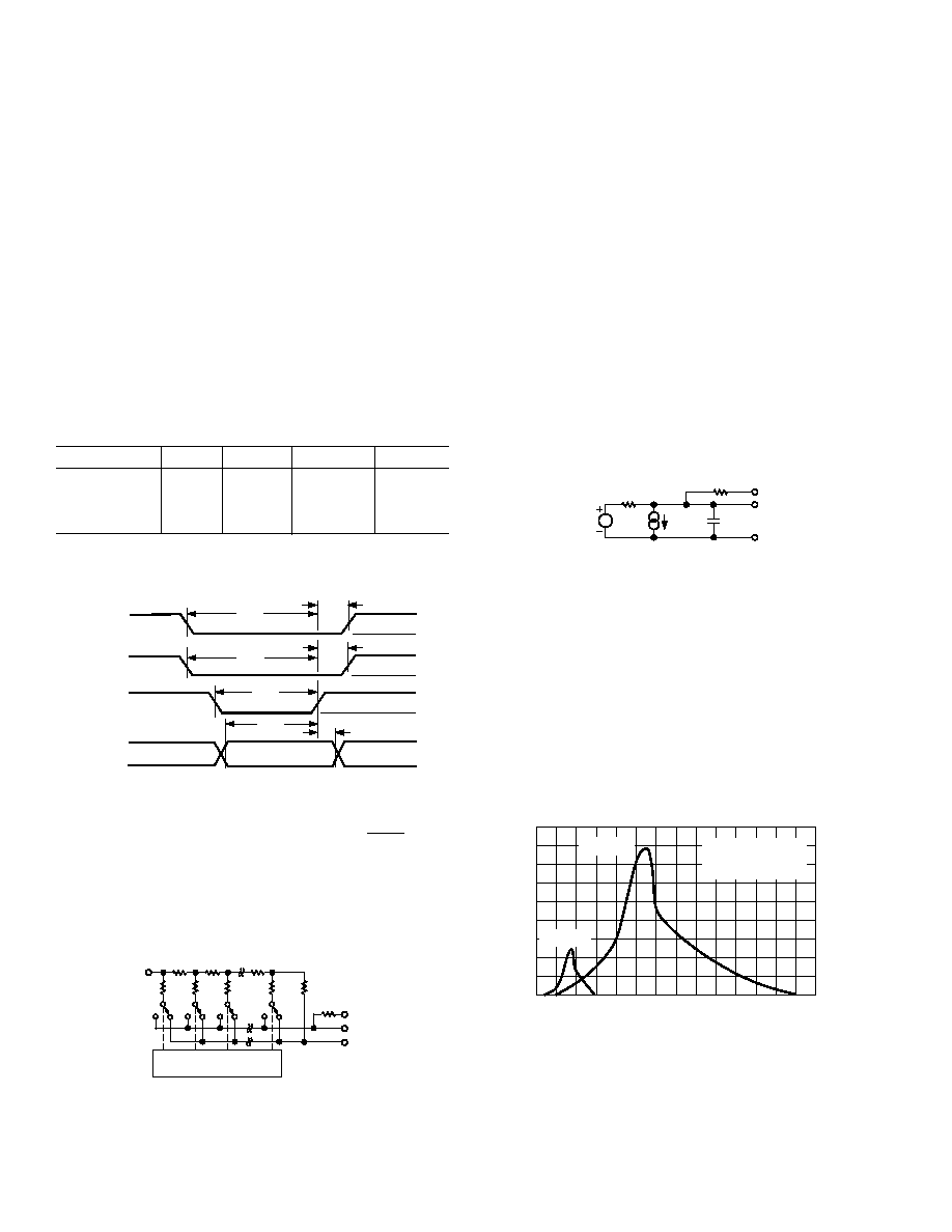
VIN – Volts
800
0
I DD
A
(V
DD
=
+5V)
1
2
3
4
5
6
7
8
9
10
11
13
14
12
700
600
500
400
300
200
100
I DD
mA
(V
DD
=
+15V)
9
8
7
6
5
4
3
2
1
VDD = +5V
VDD = +15V
TA = +25 C
ALL DIGITAL INPUTS
TIED TOGETHER
Figure 3. Typical Plots of Supply Current, IDD vs. Logic
Input Voltage VIN, for VDD = +5 V and +15 V
相关PDF资料 |
PDF描述 |
|---|---|
| VE-JN1-MZ-B1 | CONVERTER MOD DC/DC 12V 25W |
| LTC1450LIG#PBF | IC D/A CONV 12BIT R-R PAR 24SSOP |
| VE-JN0-MZ-B1 | CONVERTER MOD DC/DC 5V 25W |
| VI-JNZ-MZ-B1 | CONVERTER MOD DC/DC 2V 10W |
| LTC1450LIG | IC D/A CONV 12BIT R-R PAR 24SSOP |
相关代理商/技术参数 |
参数描述 |
|---|---|
| AD7528KR | 制造商:AD 制造商全称:Analog Devices 功能描述:CMOS Dual 8-Bit Buffered Multiplying DAC |
| AD7528LCWP | 制造商:未知厂家 制造商全称:未知厂家 功能描述:8-Bit Digital-to-Analog Converter |
| AD7528LN | 功能描述:IC DAC 8BIT DUAL MULT 20-DIP RoHS:否 类别:集成电路 (IC) >> 数据采集 - 数模转换器 系列:- 标准包装:2,400 系列:- 设置时间:- 位数:18 数据接口:串行 转换器数目:3 电压电源:模拟和数字 功率耗散(最大):- 工作温度:-40°C ~ 85°C 安装类型:表面贴装 封装/外壳:36-TFBGA 供应商设备封装:36-TFBGA 包装:带卷 (TR) 输出数目和类型:* 采样率(每秒):* |
| AD7528LN/+ | 制造商:Rochester Electronics LLC 功能描述:- Bulk |
| AD7528LNZ | 功能描述:IC DAC 8BIT DUAL MULTIPLY 20-DIP RoHS:是 类别:集成电路 (IC) >> 数据采集 - 数模转换器 系列:- 产品培训模块:Data Converter Fundamentals DAC Architectures 标准包装:750 系列:- 设置时间:7µs 位数:16 数据接口:并联 转换器数目:1 电压电源:双 ± 功率耗散(最大):100mW 工作温度:0°C ~ 70°C 安装类型:表面贴装 封装/外壳:28-LCC(J 形引线) 供应商设备封装:28-PLCC(11.51x11.51) 包装:带卷 (TR) 输出数目和类型:1 电压,单极;1 电压,双极 采样率(每秒):143k |
发布紧急采购,3分钟左右您将得到回复。