- 您现在的位置:买卖IC网 > PDF目录378276 > AD7531LN (INTERSIL CORP) 10-Bit, 12-Bit, Multiplying D/A Converters PDF资料下载
参数资料
| 型号: | AD7531LN |
| 厂商: | INTERSIL CORP |
| 元件分类: | DAC |
| 英文描述: | 10-Bit, 12-Bit, Multiplying D/A Converters |
| 中文描述: | PARALLEL, WORD INPUT LOADING, 1 us SETTLING TIME, 12-BIT DAC, PDIP18 |
| 封装: | PLASTIC, DIP-18 |
| 文件页数: | 3/14页 |
| 文件大小: | 264K |
| 代理商: | AD7531LN |
Electrical Characteristics
(V
a
e
15V, V
REF
e
10.000V, T
A
e
25
§
C unless otherwise specified) (Continued)
DAC1020, DAC1021,
DAC1022
DAC1220, DAC1222
Parameter
Conditions
Units
Min
Typ
Max
Min
Typ
Max
Digital Input
Low Threshold
High Threshold
(Figure 1)
T
MIN
k
T
A
k
T
MAX
T
MIN
k
T
A
k
T
MAX
0.8
0.8
V
V
2.4
2.4
Digital Input Current
T
MIN
s
T
A
s
T
MAX
Digital Input High
Digital Input Low
1
100
b
200
1
100
b
200
m
A
m
A
b
50
b
50
Supply Current
All Digital Inputs High
All Digital Inputs Low
0.2
0.6
1.6
2
0.2
0.6
1.6
2
mA
mA
Operating Power Supply
Range
(Figures 1 and 2)
5
15
5
15
V
Note 1:
V
REF
e
g
10V and V
REF
e
g
1V. A linearity error temperature coefficient of 0.0002% FS for a 45
§
C rise only guarantees 0.009% maximum change in
linearity error. For instance, if the linearity error at 25
§
C is 0.045% FS it could increase to 0.054% at 70
§
C and the DAC will be no longer a 10-bit part. Note,
however, that the linearity error is specified over the device full temperature range which is a more stringent specification since it includes the linearity error
temperature coefficient.
Note 2:
Using internal feedback resistor as shown in Figure 3.
Note 3:
Both I
OUT 1
and I
OUT 2
must go to ground or the virtual ground of an operational amplifier. If V
REF
e
10V, every millivolt offset between I
OUT 1
or I
OUT 2
,
0.005% linearity error will be introduced.
Note 4:
Human body model, 100 pF discharged through a 1.5 k
X
resistor.
Note 5:
Absolute Maximum Ratings indicate limits beyond which damage to the device may occur. DC and AC electrical specifications do not apply when operating
the device beyond its specified operating conditions.
Note 6:
The maximum power dissipation must be derated at elevated temperatures and is dictated by T
JMAX
,
i
JA
, and the ambient temepature, T
A
. The maximum
allowable power dissipation at any temperature is P
D
e
(T
JMAX
b
T
A
)/
i
JA
or the number given in the Absolute Maximum Ratings, whichever is lower. For this
device, T
JMAX
e
125
§
C, and the typical junction-to-ambient thermal resistance of the J18 package when board mounted is 85
§
C/W. For the N18 package,
i
JA
is
120
§
C/W, for the N16 this number is 125
§
C/W, and for the V20 this number is 95
§
C/W.
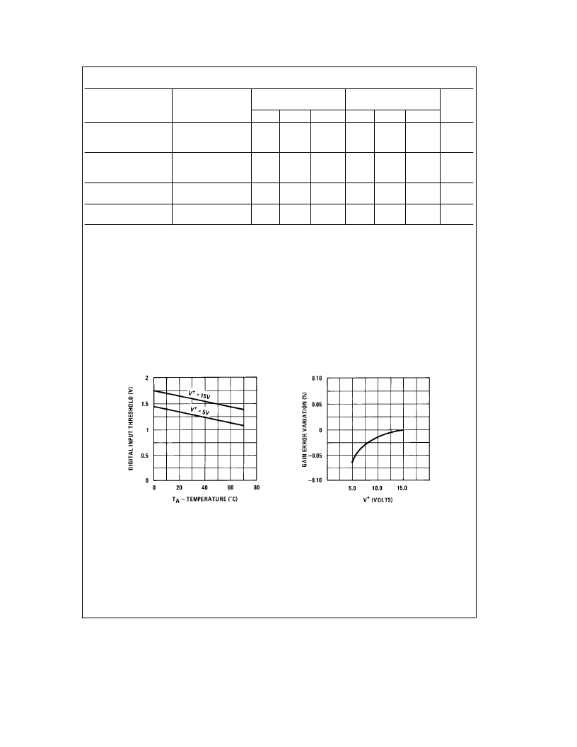
Typical Performance Characteristics
TL/H/5689–2
FIGURE 1. Digital Input Threshold vs
Ambient Temperature
FIGURE 2. Gain Error Variation vs V
a
http://www.national.com
3
相关PDF资料 |
PDF描述 |
|---|---|
| AD7531JN | 10-Bit, 12-Bit, Multiplying D/A Converters |
| AD7523 | 8-Bit, Multiplying D/A Converters |
| AD7523KN | 8-Bit, Multiplying D/A Converters |
| AD7523LN | 8-Bit, Multiplying D/A Converters |
| AD7523JN | 8-Bit, Multiplying D/A Converters |
相关代理商/技术参数 |
参数描述 |
|---|---|
| AD7531LN/A+ | 制造商:未知厂家 制造商全称:未知厂家 功能描述:12-Bit Digital-to-Analog Converter |
| AD7531LN/B+ | 制造商:未知厂家 制造商全称:未知厂家 功能描述:12-Bit Digital-to-Analog Converter |
| AD7531LQ | 制造商:未知厂家 制造商全称:未知厂家 功能描述:12-Bit Digital-to-Analog Converter |
| AD7531SD | 制造商:未知厂家 制造商全称:未知厂家 功能描述:Converter IC |
| AD7531SN | 制造商:未知厂家 制造商全称:未知厂家 功能描述:Converter IC |
发布紧急采购,3分钟左右您将得到回复。