- 您现在的位置:买卖IC网 > PDF目录10786 > AD7533JPZ-REEL (Analog Devices Inc)IC DAC 10BIT MULTIPLYING 20PLCC PDF资料下载
参数资料
| 型号: | AD7533JPZ-REEL |
| 厂商: | Analog Devices Inc |
| 文件页数: | 10/12页 |
| 文件大小: | 0K |
| 描述: | IC DAC 10BIT MULTIPLYING 20PLCC |
| 产品培训模块: | Data Converter Fundamentals DAC Architectures |
| 产品变化通告: | Product Discontinuance 27/Oct/2011 |
| 标准包装: | 1,000 |
| 设置时间: | 600ns |
| 位数: | 10 |
| 数据接口: | 并联 |
| 转换器数目: | 1 |
| 电压电源: | 单电源 |
| 功率耗散(最大): | 30mW |
| 工作温度: | -40°C ~ 85°C |
| 安装类型: | 表面贴装 |
| 封装/外壳: | 20-LCC(J 形引线) |
| 供应商设备封装: | 20-PLCC(9x9) |
| 包装: | 带卷 (TR) |
| 输出数目和类型: | 2 电流,单极;2 电流,双极 |
| 采样率(每秒): | 1.7M |
AD7533
Rev. C | Page 7 of 12
CIRCUIT DESCRIPTION
GENERAL CIRCUIT INFORMATION
The AD7533 is a 10-bit multiplying DAC that consists of a
highly stable thin-film R-2R ladder and ten CMOS current
switches on a monolithic chip. Most applications require the
addition of only an output operational amplifier and a voltage
or current reference.
The simplified D/A circuit is shown in Figure 7. An inverted
R- 2R ladder structure is used, that is, the binarily weighted
currents are switched between the IOUT1 and IOUT2 bus lines,
thus maintaining a constant current in each ladder leg
independent of the switch state.
20k
S1
S2
S3
SN
IOUT2
VREF
IOUT1
RFB
20k
10k
BIT 1 (MSB)
BIT 10 (LSB)
DIGITAL INPUTS (DTL/TTL/CMOS COMPATIBLE)
BIT 2
BIT 3
10k
20k
01134-
001
Figure 7. Functional Diagram
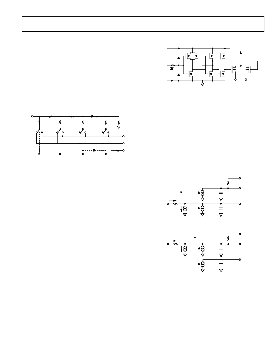
One of the CMOS current switches is shown in Figure 8. The
geometries of Device 1, Device 2, and Device 3 are optimized to
make the digital control inputs DTL/TTL/CMOS compatible
over the full military temperature range. The input stage drives
two inverters (Device 4, Device 5, Device 6, and Device 7),
which in turn drive the two output N channels. The on
resistances of the switches are binarily sealed so that the voltage
drop across each switch is the same. For example, Switch 1 in
Figure 8 is designed for an on resistance of 20 Ω, Switch 2 for
40 Ω, and so on. For a 10 V reference input, the current through
Switch 1 is 0.5 mA, the current through Switch 2 is 0.25 mA,
and so on, thus maintaining a constant 10 mV drop across each
switch. It is essential that each switch voltage drop be equal if
the binarily weighted current division property of the ladder is
to be maintained.
DTL/TTL/
CMOS
INPUT
V+
13
2
TO LADDER
5
4
250
7
6
89
IOUT1
IOUT2
01
13
4-
0
07
Figure 8. CMOS Switch
EQUIVALENT CIRCUIT ANALYSIS
The equivalent circuits for all digital inputs high and digital
all digital inputs low, the reference current is switched to IOUT2.
The current source ILEAKAGE is composed of surface and junction
leakages to the substrate, while the I/1024 current source represents
a constant 1-bit current drain through the termination resistor
on the R-2R ladder. The on capacitance of the output N channel
switch is 100 pF, as shown on the IOUT2 terminal. The off switch
capacitance is 35 pF, as shown on the IOUT1 terminal. Analysis of
the circuit for all digital inputs high, as shown in Figure 10, is
similar to Figure 9; however, the on switches are now on
Terminal IOUT1. Therefore, there is the 100 pF at that terminal.
IOUT2
IOUT1
VREF
IREF
RFB
ILEAKAGE
R
011
34
-00
8
R
10k
100pF
ILEAKAGE
35pF
I/1024
Figure 9. Equivalent Circuit—All Digital Inputs Low
IOUT2
IOUT1
VREF
IREF
RFB
ILEAKAGE
R
01
13
4-
0
9
R
100pF
ILEAKAGE
35pF
I/1024
R
10k
Figure 10. Equivalent Circuit—All Digital Inputs High
相关PDF资料 |
PDF描述 |
|---|---|
| VI-JTT-MY-S | CONVERTER MOD DC/DC 6.5V 50W |
| VI-21V-IW-S | CONVERTER MOD DC/DC 5.8V 100W |
| VI-BNT-MX-F4 | CONVERTER MOD DC/DC 6.5V 75W |
| AD7542JPZ-REEL | IC DAC 12BIT MULT CMOS 20PLCC |
| VI-BNT-MX-F2 | CONVERTER MOD DC/DC 6.5V 75W |
相关代理商/技术参数 |
参数描述 |
|---|---|
| AD7533JR | 制造商:AD 制造商全称:Analog Devices 功能描述:CMOS LOW COST 10-BIT MULTIPLYING DAC |
| AD7533KCWE | 制造商:未知厂家 制造商全称:未知厂家 功能描述:10-Bit Digital-to-Analog Converter |
| AD7533KD | 制造商:未知厂家 制造商全称:未知厂家 功能描述:Converter IC |
| AD7533KN | 功能描述:IC DAC 10BIT MULTIPLYING 16-DIP RoHS:否 类别:集成电路 (IC) >> 数据采集 - 数模转换器 系列:- 标准包装:47 系列:- 设置时间:2µs 位数:14 数据接口:并联 转换器数目:1 电压电源:单电源 功率耗散(最大):55µW 工作温度:-40°C ~ 85°C 安装类型:表面贴装 封装/外壳:28-SSOP(0.209",5.30mm 宽) 供应商设备封装:28-SSOP 包装:管件 输出数目和类型:1 电流,单极;1 电流,双极 采样率(每秒):* |
| AD7533KN/+ | 制造商:Rochester Electronics LLC 功能描述:- Bulk |
发布紧急采购,3分钟左右您将得到回复。