参数资料
| 型号: | AD7537KN |
| 厂商: | Analog Devices Inc |
| 文件页数: | 6/10页 |
| 文件大小: | 0K |
| 描述: | IC DAC 12BIT LC2MOS DUAL 24-DIP |
| 产品培训模块: | Data Converter Fundamentals DAC Architectures |
| 标准包装: | 15 |
| 设置时间: | 250µs |
| 位数: | 12 |
| 数据接口: | 并联 |
| 转换器数目: | 2 |
| 电压电源: | 单电源 |
| 功率耗散(最大): | 24mW |
| 工作温度: | -40°C ~ 85°C |
| 安装类型: | 通孔 |
| 封装/外壳: | 24-DIP(0.300",7.62mm) |
| 供应商设备封装: | 24-PDIP |
| 包装: | 管件 |
| 输出数目和类型: | 2 电流,单极;2 电流,双极 |
| 采样率(每秒): | 667k |
AD7537
REV.
–5–
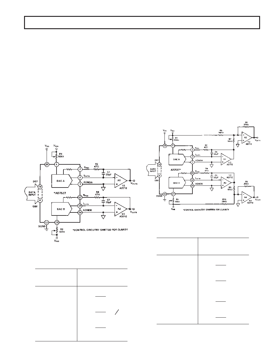
UNIPOLAR BINARY OPERATION
(2-QUADRANT MULTIPLICATION)
Figure 4 shows the circuit diagram for unipolar binary opera-
tion. With an ac input, the circuit performs 2-quadrant multipli-
cation. The code table for Figure 4 is given in Table II.
Operational amplifiers A1 and A2 can be in a single package
(AD644, AD712) or separate packages (AD544, AD711,
AD OP27). Capacitors C1 and C2 provide phase compensation
to help prevent overshoot and ringing when high-speed op amps
are used.
For zero offset adjustment, the appropriate DAC register is
loaded with all 0s and amplifier offset adjusted so that VOUTA or
VOUTB is 0 V. Full-scale trimming is accomplished by loading
the DAC register with all 1s and adjusting R1 (R3) so that
VOUTA (VOUTB) = –VIN (4095/4096). For high temperature op-
eration, resistors and potentiometers should have a low Tem-
perature Coefficient. In many applications, because of the
excellent Gain T.C. and Gain Error specifications of the
AD7537, Gain Error trimming is not necessary. In fixed refer-
ence applications, full scale can also be adjusted by omitting R1,
R2, R3, R4 and trimming the reference voltage magnitude.
Figure 4. AD7537 Unipolar Binary Operation
Table II. Unipolar Binary Code Table for
Circuit of Figure 4
Binary Number in
DAC Register
Analog Output,
MSB
LSB
VOUTA or VOUTB
1111 1111 1111
V
IN
4095
4096
1000 0000 0000
V
IN
2048
4096
= 1
2 V IN
0000 0000 0001
V
IN
1
4096
0000 0000 0000
0 V
BIPOLAR OPERATION
(4-QUADRANT MULTIPLICATION)
The recommended circuit diagram for bipolar operation is
shown in Figure 5. Offset binary coding is used.
With the appropriate DAC register loaded to 1000 0000 0000,
adjust R1 (R3) so that VOUTA (VOUTB) = 0 V. Alternatively, R1,
R2 (R3, R4) may be omitted and the ratios of R6, R7 (R9, 10)
varied for VOUTA (VOUTB) = 0 V. Full-scale trimming can be ac-
complished by adjusting the amplitude of VIN or by varying the
value of R5 (R8).
If R1, R2 (R3, R4) are not used, then resistors R5, R6, R7 (R8,
R9, R10) should be ratio matched to 0.01% to ensure gain error
performance to the data sheet specification. When operating
over a wide temperature range, it is important that the resistors
be of the same type so that their temperature coefficients match.
The code table for Figure 5 is given in Table III.
Figure 5. Bipolar Operation (Offset Binary Coding)
Table III. Bipolar Code Table for Offset Binary
Circuit of Figure 5
Binary Number in
DAC Register
Analog Output,
MSB
LSB
VOUTA or VOUTB
1111 1111 1111
+V
IN
2047
2048
1000 0000 0001
+V
IN
1
2048
1000 0000 0000
0 V
0111 1111 1111
V
IN
1
2048
0000 0000 0000
V
IN
2048
=V
IN
Applications–
A
相关PDF资料 |
PDF描述 |
|---|---|
| LTC2757BCLX#PBF | IC DAC 18BIT PAR 48LQFP |
| AD767KPZ | IC DAC 12BIT W/AMP 28-PLCC |
| AD5392BCPZ-5 | IC DAC 14BIT 8CHAN 5V 64LFCSP |
| AD5570BRSZ-REEL7 | IC DAC 16BIT SERIAL IN 16SSOP |
| AD5570BRSZ-REEL | IC DAC 16BIT SERIAL IN 16SSOP |
相关代理商/技术参数 |
参数描述 |
|---|---|
| AD7537KN/+ | 制造商:未知厂家 制造商全称:未知厂家 功能描述:12-Bit Digital-to-Analog Converter |
| AD7537KNZ | 功能描述:IC DAC 12BIT DUAL MULT 24DIP RoHS:是 类别:集成电路 (IC) >> 数据采集 - 数模转换器 系列:- 产品培训模块:Data Converter Fundamentals DAC Architectures 标准包装:750 系列:- 设置时间:7µs 位数:16 数据接口:并联 转换器数目:1 电压电源:双 ± 功率耗散(最大):100mW 工作温度:0°C ~ 70°C 安装类型:表面贴装 封装/外壳:28-LCC(J 形引线) 供应商设备封装:28-PLCC(11.51x11.51) 包装:带卷 (TR) 输出数目和类型:1 电压,单极;1 电压,双极 采样率(每秒):143k |
| AD7537KP | 功能描述:IC DAC 12BIT LC2MOS DUAL 28-PLCC RoHS:否 类别:集成电路 (IC) >> 数据采集 - 数模转换器 系列:- 产品培训模块:Data Converter Fundamentals DAC Architectures 标准包装:750 系列:- 设置时间:7µs 位数:16 数据接口:并联 转换器数目:1 电压电源:双 ± 功率耗散(最大):100mW 工作温度:0°C ~ 70°C 安装类型:表面贴装 封装/外壳:28-LCC(J 形引线) 供应商设备封装:28-PLCC(11.51x11.51) 包装:带卷 (TR) 输出数目和类型:1 电压,单极;1 电压,双极 采样率(每秒):143k |
| AD7537KPZ | 功能描述:IC DAC 12BIT LC2MOS DUAL 28-PLCC RoHS:是 类别:集成电路 (IC) >> 数据采集 - 数模转换器 系列:- 标准包装:1 系列:- 设置时间:4.5µs 位数:12 数据接口:串行,SPI? 转换器数目:1 电压电源:单电源 功率耗散(最大):- 工作温度:-40°C ~ 125°C 安装类型:表面贴装 封装/外壳:8-SOIC(0.154",3.90mm 宽) 供应商设备封装:8-SOICN 包装:剪切带 (CT) 输出数目和类型:1 电压,单极;1 电压,双极 采样率(每秒):* 其它名称:MCP4921T-E/SNCTMCP4921T-E/SNRCTMCP4921T-E/SNRCT-ND |
| AD7537KPZ-REEL | 制造商:AD 制造商全称:Analog Devices 功能描述:LC2MOS 84) Loading Dual 12-Bit DAC |
发布紧急采购,3分钟左右您将得到回复。