参数资料
| 型号: | AD7538KR |
| 厂商: | Analog Devices Inc |
| 文件页数: | 3/16页 |
| 文件大小: | 0K |
| 描述: | IC DAC 14BIT W/BUFF 24-SOIC |
| 产品培训模块: | Data Converter Fundamentals DAC Architectures |
| 标准包装: | 1 |
| 设置时间: | 1.5µs |
| 位数: | 14 |
| 数据接口: | 并联 |
| 转换器数目: | 1 |
| 电压电源: | 单电源 |
| 功率耗散(最大): | 1W |
| 工作温度: | 0°C ~ 70°C |
| 安装类型: | 表面贴装 |
| 封装/外壳: | 24-SOIC(0.295",7.50mm 宽) |
| 供应商设备封装: | 24-SOIC W |
| 包装: | 管件 |
| 输出数目和类型: | 1 电流,单极;1 电流,双极 |
| 采样率(每秒): | 667k |
AD7538
Rev. B | Page 11 of 16
BIPOLAR OPERATION (4-QUADRANT
MULTIPLICATION)
The recommended circuit diagram for bipolar operation is
shown in Figure 8. Offset binary coding is used. The code table
With the DAC loaded to 10 0000 0000 0000, adjust R1 for VO =
0 V. Alternatively, one can omit R1 and R2 and adjust the ratio
of R5 and R6 for VO = 0 V. Full-scale trimming can be accom-
plished by adjusting the amplitude of VIN or by varying the
value of R7.
The values given for R1, R2 are the minimum necessary to
calibrate the system for Resistors R5, R6, R7 ratio matched to
0.1%. System linearity error is independent of resistor ratio
matching and is affected by DAC linearity error only.
When operating over a wide temperature range, it is important
that the resistors be of the same type so that their temperature
coefficients match.
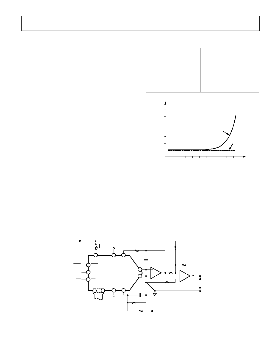
LOW LEAKAGE CONFIGURATION
For CMOS multiplying DAC, as the device is operated at higher
temperatures, the output leakage current increases. For a 14-bit
resolution system, this can be a significant source of error. The
AD7538 features a leakage reduction configuration to keep the
leakage current low over an extended temperature range. One
may operate the device with or without this configuration. If VSS
(Pin 24) is tied to AGND then the DAC exhibits normal output
leakage currents at high temperatures. To use the low leakage
facility, VSS should be tied to a voltage of approximately 0.3 V
as in Figure 6 and Figure 8. A simple resistor divider (R3, R4)
produces approximately 300 mV from 15 V. The C2
capacitor in parallel with R3 is an integral part of the low
leakage configuration and must be 4.7 μF or greater. Figure 7
is a plot of leakage current vs. temperature for both conditions.
It clearly shows the improvement gained by using the low
leakage configuration.
Table 7. Bipolar Code Table for the Offset Binary Circuit
of Figure 8
Binary Number In
DAC Register
Analog Output VOUT
MSB
LSB
11 1111 1111 1111
+VIN(8191/8192)
10 0000 0000 0001
+VIN(1/8192)
10 0000 0000 0000
0 V
01 1111 1111 1111
VIN(1/8192)
00 0000 0000 0000
VIN(8191/8192)
30
40
50
60
70
80
90
100 110 120
TEMPERATURE (°C)
L
E
AKA
G
E
CURR
E
NT
(n
A)
60
50
40
30
20
10
0
VDD = 15V
VREF = 10V
VSS = 0V
VSS = –0.3V
0
1
13
9-
0
08
Figure 7. Graph of Typical Leakage Current vs. Temperature for AD7538
619
5
24
23
1
20
21
22
2
3
4
DB13 TO DB0 DGND
VDD
VREF
RFB
IOUT
VDD
–15V
AGND
VSS
LDAC
CS
WR
LDAC
CS
WR
AD7538
A1
R3
1k
R2
22
R5
10k
R7
20k
R6
20k
R8
5k, 10%
R1
50
R4
47k
INPUT DATA
DIGITAL
GND
C2
4.7F
C1
33pF
ANALOG
GND
AD711
A2
AD711
01
13
9-
00
7
VIN
VO
+
Figure 8. Bipolar Operation
相关PDF资料 |
PDF描述 |
|---|---|
| MAX9512ATE+T | IC VIDEO FILTER AMP 16-TQFN |
| VI-23X-IV-F2 | CONVERTER MOD DC/DC 5.2V 150W |
| VI-B5L-MU | CONVERTER MOD DC/DC 28V 200W |
| VI-23V-IV-F2 | CONVERTER MOD DC/DC 5.8V 150W |
| VI-23T-IV-F1 | CONVERTER MOD DC/DC 6.5V 150W |
相关代理商/技术参数 |
参数描述 |
|---|---|
| AD7538KR-REEL | 制造商:Analog Devices 功能描述: |
| AD7538KRZ | 功能描述:IC DAC 14BIT W/BUFF 24-SOIC RoHS:是 类别:集成电路 (IC) >> 数据采集 - 数模转换器 系列:- 标准包装:1 系列:- 设置时间:4.5µs 位数:12 数据接口:串行,SPI? 转换器数目:1 电压电源:单电源 功率耗散(最大):- 工作温度:-40°C ~ 125°C 安装类型:表面贴装 封装/外壳:8-SOIC(0.154",3.90mm 宽) 供应商设备封装:8-SOICN 包装:剪切带 (CT) 输出数目和类型:1 电压,单极;1 电压,双极 采样率(每秒):* 其它名称:MCP4921T-E/SNCTMCP4921T-E/SNRCTMCP4921T-E/SNRCT-ND |
| AD7538KRZ1 | 制造商:AD 制造商全称:Analog Devices 功能描述:LC2MOS Microprocessor-Compatible 14-Bit DAC |
| AD7538KRZ-REEL | 功能描述:IC DAC 14BIT W/BUFF 24-SOIC RoHS:是 类别:集成电路 (IC) >> 数据采集 - 数模转换器 系列:- 标准包装:2,400 系列:- 设置时间:- 位数:18 数据接口:串行 转换器数目:3 电压电源:模拟和数字 功率耗散(最大):- 工作温度:-40°C ~ 85°C 安装类型:表面贴装 封装/外壳:36-TFBGA 供应商设备封装:36-TFBGA 包装:带卷 (TR) 输出数目和类型:* 采样率(每秒):* |
| AD7538KRZ-REEL1 | 制造商:AD 制造商全称:Analog Devices 功能描述:LC2MOS Microprocessor-Compatible 14-Bit DAC |
发布紧急采购,3分钟左右您将得到回复。