参数资料
| 型号: | AD7541AJNZ |
| 厂商: | Analog Devices Inc |
| 文件页数: | 5/8页 |
| 文件大小: | 0K |
| 描述: | IC DAC 12BIT MULT MONO 18-DIP |
| 产品培训模块: | Data Converter Fundamentals DAC Architectures |
| 标准包装: | 20 |
| 设置时间: | 600ns |
| 位数: | 12 |
| 数据接口: | 并联 |
| 转换器数目: | 1 |
| 电压电源: | 单电源 |
| 工作温度: | 0°C ~ 70°C |
| 安装类型: | 通孔 |
| 封装/外壳: | 18-DIP(0.300",7.62mm) |
| 供应商设备封装: | 18-PDIP |
| 包装: | 管件 |
| 输出数目和类型: | 2 电流,单极;2 电流,双极 |
| 采样率(每秒): | * |
| 产品目录页面: | 784 (CN2011-ZH PDF) |
AD7541A
–5–
REV. B
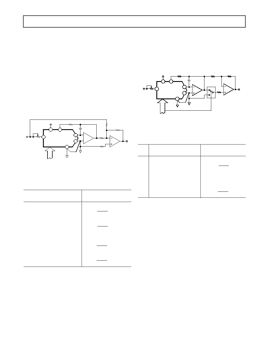
BIPOLAR OPERATION
(4-QUADRANT MULTIPLICATION)
Figure 5 and Table III illustrate the circuitry and code relation-
ship for bipolar operation. With a dc reference (positive or nega-
tive polarity) the circuit provides offset binary operation. With
an ac reference the circuit provides full 4-quadrant multiplication.
With the DAC loaded to 1000 0000 0000, adjust R1 for
VOUT = 0 V (alternatively, one can omit R1 and R2 and adjust
the ratio of R3 to R4 for VOUT = 0 V). Full-scale trimming can
be accomplished by adjusting the amplitude of VREF or by vary-
ing the value of R5.
As in unipolar operation, A1 must be chosen for low VOS and
low IB. R3, R4 and R5 must be selected for matching and track-
ing. Mismatch of 2R3 to R4 causes both offset and full-scale
error. Mismatch of R5 to R4 or 2R3 causes full-scale error. C1
phase compensation (10 pF to 50 pF) may be required for sta-
bility, depending on amplifier used.
AD7541A
A1
3
R2
*
VDD
16
17
18
1
2
VDD
RFB
VREF
PINS 4–15
GND
OUT1
OUT2
R1
*
VIN
BIT 1 – BIT 12
DIGITAL
GROUND
ANALOG
COMMON
C1
33pF
AD544L
VOUT
AD544J
A2
R4
20k
R5
20k
R3
10k
R6
5k
10%
*FOR VALUES OF R1 AND R2
SEE TABLE 1.
Figure 5. Bipolar Operation (4-Quadrant Multiplication)
Table III. Bipolar Code Table for Offset Binary Circuit of
Figure 5
Binary Number in DAC
MSB
LSB
Analog Output, VOUT
1 1 1 1
+VIN
2047
2048
1 0 0 0
0 0 0 0
0 0 0 1
+VIN
1
2048
1 0 0 0
0 0 0 0
0 Volts
0 1 1 1
1 1 1 1
–VIN
1
2048
0 0 0 0
–VIN
2048
Figure 6 and Table IV show an alternative method of achieving
bipolar output. The circuit operates with sign plus magnitude
code and has the advantage of giving 12-bit resolution in each
quadrant, compared with 11-bit resolution per quadrant for the
circuit of Figure 5. The AD7592 is a fully protected CMOS
changeover switch with data latches. R4 and R5 should match
each other to 0.01% to maintain the accuracy of the D/A con-
verter. Mismatch between R4 and R5 introduces a gain error.
A2
AD7541A
A1
3
R2
*
VDD
16
17
18
1
2
VDD
RFB
VREF
PINS 4–15
GND
OUT1
OUT2
R1
*
VIN
BIT 1 – BIT 12
DIGITAL
GROUND
ANALOG
COMMON
C1
33pF
AD544L
VOUT
AD544J
R5
20k
*FOR VALUES OF R1 AND R2
SEE TABLE 1.
R4
20k
R3
10k
10%
1/2 AD7592JN
SIGN BIT
Figure 6. 12-Bit Plus Sign Magnitude Operation
Table IV. 12-Bit Plus Sign Magnitude Code Table for Circuit
of Figure 6
Sign
Binary Number in DAC
Bit
MSB
LSB
Analog Output, VOUT
0
1 1 1 1
+VIN
×
4095
4096
0
0 0 0 0
0 Volts
1
0 0 0 0
0 Volts
1
1 1 1 1 1 1 1 1
1 1 1 1
–VIN ×
4095
4096
Note: Sign bit of “0” connects R3 to GND.
相关PDF资料 |
PDF描述 |
|---|---|
| VI-BVV-MY-F4 | CONVERTER MOD DC/DC 5.8V 50W |
| VI-BVV-MY-F3 | CONVERTER MOD DC/DC 5.8V 50W |
| VI-BVX-MY-F4 | CONVERTER MOD DC/DC 5.2V 50W |
| VI-BVX-MY-F2 | CONVERTER MOD DC/DC 5.2V 50W |
| AD1853JRSZ | IC DAC STEREO 24BIT 28SSOP |
相关代理商/技术参数 |
参数描述 |
|---|---|
| AD7541AJNZ | 制造商:Analog Devices 功能描述:D/A Converter (D-A) IC |
| AD7541AJNZ-MOOG | 制造商:Analog Devices 功能描述: |
| AD7541AJP | 制造商:Analog Devices 功能描述:DAC 1-CH R-2R 12-bit 20-Pin PLCC 制造商:Rochester Electronics LLC 功能描述:CMOS MONOLITHIC IC - Bulk |
| AD7541AJP-REEL | 功能描述:IC DAC 12BIT MULT MONO 20-PLCC RoHS:否 类别:集成电路 (IC) >> 数据采集 - 数模转换器 系列:- 标准包装:2,400 系列:- 设置时间:- 位数:18 数据接口:串行 转换器数目:3 电压电源:模拟和数字 功率耗散(最大):- 工作温度:-40°C ~ 85°C 安装类型:表面贴装 封装/外壳:36-TFBGA 供应商设备封装:36-TFBGA 包装:带卷 (TR) 输出数目和类型:* 采样率(每秒):* |
| AD7541AJPZ | 功能描述:IC DAC 12BIT MULT MONO 20PLCC RoHS:是 类别:集成电路 (IC) >> 数据采集 - 数模转换器 系列:- 标准包装:2,400 系列:- 设置时间:- 位数:18 数据接口:串行 转换器数目:3 电压电源:模拟和数字 功率耗散(最大):- 工作温度:-40°C ~ 85°C 安装类型:表面贴装 封装/外壳:36-TFBGA 供应商设备封装:36-TFBGA 包装:带卷 (TR) 输出数目和类型:* 采样率(每秒):* |
发布紧急采购,3分钟左右您将得到回复。