参数资料
| 型号: | AD7541AKNZ |
| 厂商: | Analog Devices Inc |
| 文件页数: | 3/8页 |
| 文件大小: | 0K |
| 描述: | IC DAC 12BIT MULT MONO 18-DIP |
| 产品培训模块: | Data Converter Fundamentals DAC Architectures |
| 标准包装: | 20 |
| 设置时间: | 600ns |
| 位数: | 12 |
| 数据接口: | 并联 |
| 转换器数目: | 1 |
| 电压电源: | 单电源 |
| 工作温度: | 0°C ~ 70°C |
| 安装类型: | 通孔 |
| 封装/外壳: | 18-DIP(0.300",7.62mm) |
| 供应商设备封装: | 18-PDIP |
| 包装: | 管件 |
| 输出数目和类型: | 2 电流,单极;2 电流,双极 |
| 采样率(每秒): | * |
| 产品目录页面: | 784 (CN2011-ZH PDF) |
AD7541A
–3–
REV. B
ABSOLUTE MAXIMUM RATINGS*
(TA = +25
°C unless otherwise noted)
VDD to GND . . . . . . . . . . . . . . . . . . . . . . . . . . . . . . . . +17 V
VREF to GND . . . . . . . . . . . . . . . . . . . . . . . . . . . . . . . .
±25 V
VRFB to GND . . . . . . . . . . . . . . . . . . . . . . . . . . . . . . . . .
±25 V
Digital Input Voltage to GND . . . . . . . . –0.3 V, VDD + 0.3 V
OUT 1, OUT 2 to GND . . . . . . . . . . . . –0.3 V, VDD + 0.3 V
Power Dissipation (Any Package)
To +75
°C . . . . . . . . . . . . . . . . . . . . . . . . . . . . . . . 450 mW
Derates above +75
°C . . . . . . . . . . . . . . . . . . . . . . 6 mW/°C
TERMINOLOGY
RELATIVE ACCURACY
Relative accuracy or endpoint nonlinearity is a measure of the
maximum deviation from a straight line passing through the
endpoints of the DAC transfer function. It is measured after
adjusting for zero and full scale and is expressed in % of full-
scale range or (sub)multiples of 1 LSB.
DIFFERENTIAL NONLINEARITY
Differential nonlinearity is the difference between the measured
change and the ideal l LSB change between any two adjacent
codes. A specified differential nonlinearity of
±1 LSB max over
the operating temperature range insures monotonicity.
GAIN ERROR
Gain error is a measure of the output error between an ideal
DAC and the actual device output. For the AD7541A, ideal
maximum output is
–
4095
4096
(VREF ).
Gain error is adjustable to zero using external trims as shown in
Figures 4, 5 and 6.
OUTPUT LEAKAGE CURRENT
Current which appears at OUTI with the DAC loaded to all 0s
or at OUT2 with the DAC loaded to all 1s.
MULTIPLYING FEEDTHROUGH ERROR
AC error due to capacitive feedthrough from VREF terminal to
OUT1 with DAC loaded to all 0s.
OUTPUT CURRENT SETTLING TIME
Time required for the output function of the DAC to settle to
within 1/2 LSB for a given digital input stimulus, i.e., 0 to full
scale.
PROPAGATION DELAY
This is a measure of the internal delay of the circuit and is mea-
sured from the time a digital input changes to the point at which
the analog output at OUT1 reaches 90% of its final value.
DIGITAL-TO-ANALOG CHARGE INJECTION (QDA)
This is a measure of the amount of charge injected from the
digital inputs to the analog outputs when the inputs change
state. It is usually specified as the area of the glitch in nV secs
and is measured with VREF = GND and a Model 50K as the
output op amp, C1 (phase compensation) = 0 pF.
Operating Temperature Range
Commercial (J, K Versions) . . . . . . . . . . . . . 0
°C to +70°C
Industrial (A, B Versions) . . . . . . . . . . . . . –25
°C to +85°C
Extended (S, T Versions) . . . . . . . . . . . . . –55
°C to +125°C
Storage Temperature . . . . . . . . . . . . . . . . . . –65
°C to +150°C
Lead Temperature (Soldering, 10 secs) . . . . . . . . . . . +300
°C
*Stresses above those listed under Absolute Maximum Ratings may cause perma-
nent damage to the device. This is a stress rating only; functional operation of the
device at these or any other conditions above those indicated in the operational
sections of this specification is not implied. Exposure to absolute maximum rating
conditions for extended periods may affect device reliability.
WARNING!
ESD SENSITIVE DEVICE
CAUTION
ESD (electrostatic discharge) sensitive device. Electrostatic charges as high as 4000 V readily
accumulate on the human body and test equipment and can discharge without detection.
Although the AD7541A features proprietary ESD protection circuitry, permanent damage may
occur on devices subjected to high energy electrostatic discharges. Therefore, proper ESD
precautions are recommended to avoid performance degradation or loss of functionality.
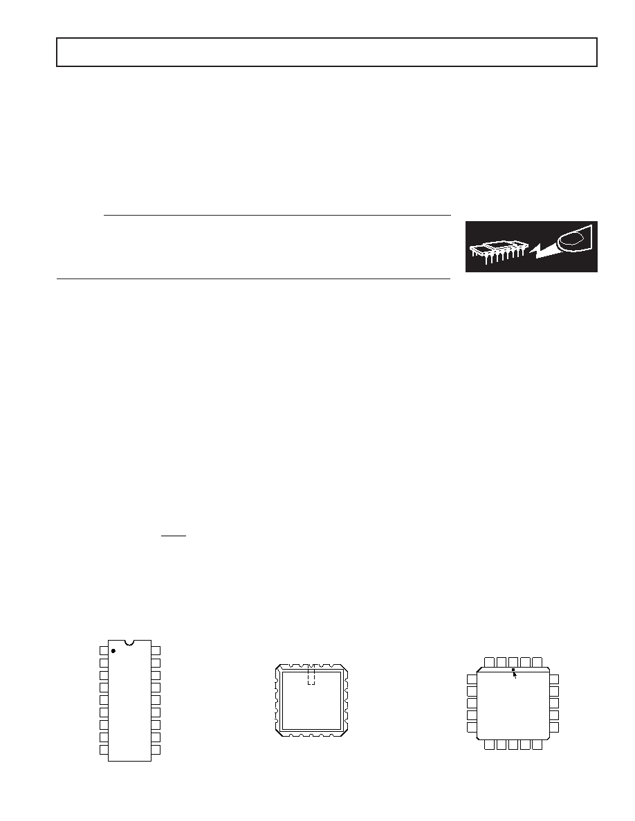
PIN CONFIGURATIONS
DIP/SOIC
LCCC
PLCC
14
13
12
11
17
16
15
18
10
9
8
1
2
3
4
7
6
5
TOP VIEW
(Not to Scale)
AD7541A
OUT1
BIT 12 (LSB)
VDD (+)
VREF IN
RFEEDBACK
OUT2
GND
BIT 1 (MSB)
BIT 9
BIT 10
BIT 11
BIT 2
BIT 3
BIT 4
BIT 5
BIT 6
BIT 7
BIT 8
20 19
1
2
3
OUT
2
OUT
1
NC
R
FB
V
REF
BIT
5
BIT
6
18
14
15
16
17
4
5
6
7
8
9 1011 1213
TOP VIEW
(Not to Scale)
AD7541A
GND
BIT 1 (MSB)
BIT 2
BIT 3
BIT 4
VDD
BIT 12 (LSB)
BIT 11
BIT 10
BIT 9
NC = NO CONNECT
NC
BIT
7
BIT
8
20 19
18
1
2
3
4
5
6
7
8
910
11 12 13
14
15
16
17
TOP VIEW
(Not to Scale)
PIN 1
IDENTIFIER
GND
BIT 1 (MSB)
BIT 2
BIT 3
BIT 4
VDD
BIT 12 (LSB)
BIT 11
BIT 10
BIT 9
NC = NO CONNECT
OUT
2
OUT
1
NC
R
FB
V
REF
AD7541A
BIT
5
BIT
6
NC
BIT
7
BIT
8
相关PDF资料 |
PDF描述 |
|---|---|
| SI5338H-A-GM | IC CLK GEN I2C BUS PROG 24QFN |
| MS3454W14S-9S | CONN RCPT 2POS JAM NUT W/SCKT |
| SI5338E-A-GM | IC CLK GEN I2C BUS PROG 24QFN |
| JN1KS10PL2 | CONN RCPT 10POS W/O PIN WALL MT |
| MS27468E17A55S | CONN RCPT 55POS JAM NUT W/SCKT |
相关代理商/技术参数 |
参数描述 |
|---|---|
| AD7541AKNZ | 制造商:Analog Devices 功能描述:IC CMOS MONOLITHIC |
| AD7541AKP | 制造商:Analog Devices 功能描述:DAC 1-CH R-2R 12-bit 20-Pin PLCC 制造商:Rochester Electronics LLC 功能描述:CMOS MONOLITHIC IC - Bulk |
| AD7541AKP-REEL | 功能描述:IC DAC 12BIT MULT MONO 20-PLCC RoHS:否 类别:集成电路 (IC) >> 数据采集 - 数模转换器 系列:- 标准包装:2,400 系列:- 设置时间:- 位数:18 数据接口:串行 转换器数目:3 电压电源:模拟和数字 功率耗散(最大):- 工作温度:-40°C ~ 85°C 安装类型:表面贴装 封装/外壳:36-TFBGA 供应商设备封装:36-TFBGA 包装:带卷 (TR) 输出数目和类型:* 采样率(每秒):* |
| AD7541AKPZ | 功能描述:IC DAC 12BIT MULT MONO 20PLCC RoHS:是 类别:集成电路 (IC) >> 数据采集 - 数模转换器 系列:- 产品培训模块:Data Converter Fundamentals DAC Architectures 标准包装:750 系列:- 设置时间:7µs 位数:16 数据接口:并联 转换器数目:1 电压电源:双 ± 功率耗散(最大):100mW 工作温度:0°C ~ 70°C 安装类型:表面贴装 封装/外壳:28-LCC(J 形引线) 供应商设备封装:28-PLCC(11.51x11.51) 包装:带卷 (TR) 输出数目和类型:1 电压,单极;1 电压,双极 采样率(每秒):143k |
| AD7541AKPZ-REEL | 功能描述:IC DAC 12BIT MULT MONO 20PLCC RoHS:是 类别:集成电路 (IC) >> 数据采集 - 数模转换器 系列:- 标准包装:47 系列:- 设置时间:2µs 位数:14 数据接口:并联 转换器数目:1 电压电源:单电源 功率耗散(最大):55µW 工作温度:-40°C ~ 85°C 安装类型:表面贴装 封装/外壳:28-SSOP(0.209",5.30mm 宽) 供应商设备封装:28-SSOP 包装:管件 输出数目和类型:1 电流,单极;1 电流,双极 采样率(每秒):* |
发布紧急采购,3分钟左右您将得到回复。