参数资料
| 型号: | AD7541AKRZ |
| 厂商: | Analog Devices Inc |
| 文件页数: | 6/8页 |
| 文件大小: | 0K |
| 描述: | IC DAC 12BIT MULT MONO 18-SOIC |
| 产品培训模块: | Data Converter Fundamentals DAC Architectures |
| 标准包装: | 41 |
| 设置时间: | 600ns |
| 位数: | 12 |
| 数据接口: | 并联 |
| 转换器数目: | 1 |
| 电压电源: | 单电源 |
| 工作温度: | 0°C ~ 70°C |
| 安装类型: | 表面贴装 |
| 封装/外壳: | 18-SOIC(0.295",7.50mm 宽) |
| 供应商设备封装: | 18-SOIC |
| 包装: | 管件 |
| 输出数目和类型: | 2 电流,单极;2 电流,双极 |
| 采样率(每秒): | * |
| 产品目录页面: | 785 (CN2011-ZH PDF) |
AD7541A
–6–
REV. B
APPLICATIONS HINTS
Output Offset: CMOS D/A converters exhibit a code-dependent
output resistance which in turn can cause a code-dependent
error voltage at the output of the amplifier. The maximum am-
plitude of this offset, which adds to the D/A converter nonlin-
earity, is 0.67 VOS where VOS is the amplifier input offset
voltage. To maintain monotonic operation it is recommended
that VOS be no greater than (25
× 10–6) (V
REF) over the tempera-
ture range of operation. Suitable op amps are AD517L and
AD544L. The AD517L is best suited for fixed reference appli-
cations with low bandwidth requirements: it has extremely low
offset (50
V) and in most applications will not require an offset
trim. The AD544L has a much wider bandwidth and higher
slew rate and is recommended for multiplying and other appli-
cations requiring fast settling. An offset trim on the AD544L
may be necessary in some circuits.
Digital Glitches: One cause of digital glitches is capacitive
coupling from the digital lines to the OUT1 and OUT2 termi-
nals. This should be minimized by screening the analog pins of
the AD7541A (Pins 1, 2, 17, 18) from the digital pins by a
ground track run between Pins 2 and 3 and between Pins 16
and 17 of the AD7541A. Note how the analog pins are at one
end of the package and separated from the digital pins by VDD
and GND to aid screening at the board level. On-chip capacitive
coupling can also give rise to crosstalk from the digital-to-analog
sections of the AD7541A, particularly in circuits with high cur-
rents and fast rise and fall times.
Temperature Coefficients: The gain temperature coefficient
of the AD7541A has a maximum value of 5 ppm/
°C and a typi-
cal value of 2 ppm/
°C. This corresponds to worst case gain shifts
of 2 LSBs and 0.8 LSBs, respectively, over a 100
°C temperature
range. When trim resistors R1 and R2 are used to adjust full-
scale range, the temperature coefficient of R1 and R2 should
also be taken into account. The reader is referred to Analog
Devices Application Note “Gain Error and Gain Temperature
Coefficient of CMOS Multiplying DACs,” Publication Number
E630c-5-3/86.
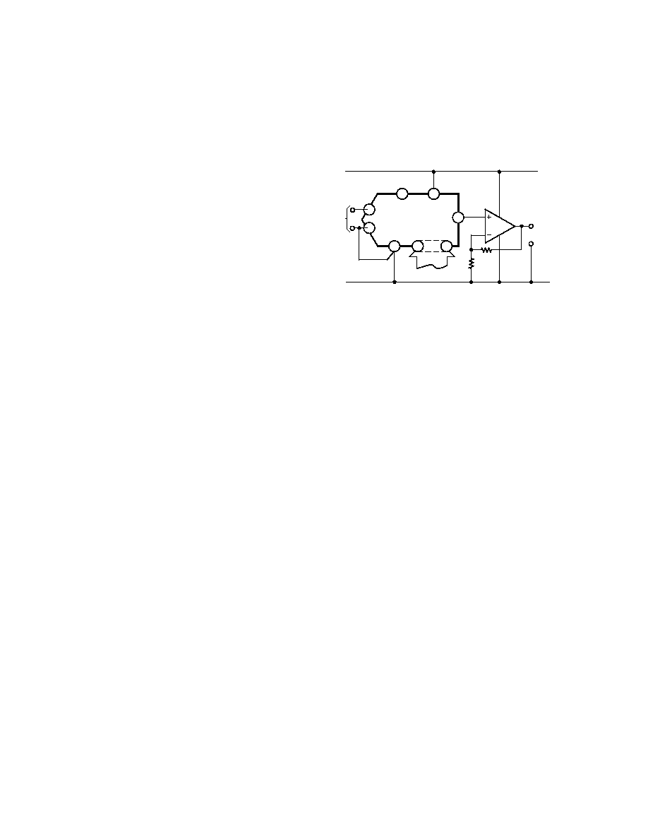
SINGLE SUPPLY OPERATION
Figure 7 shows the AD7541A connected in a voltage switching
mode. OUT1 is connected to the reference voltage and OUT2
is connected to GND. The D/A converter output voltage is
available at the VREF pin (Pin 17) and has a constant output
impedance equal to RLDR. The feedback resistor RFB is not used
in this circuit.
1
2
PINS 4–15
AD7541A
RFB
VREF
GND
OUT1
OUT2
BIT 1 – BIT 12
16
18
17
3
NOT
USED
VDD
VOUT = 0V TO +10V
R2
30k
R1
10k
SYSTEM
GROUND
V+
V–
CA3140B
VDD = +15V
VREF
+2.5V
VOUT ±VREF D (1 +R2/R1) WHERE 0 ≤ D ≤ 1
i.e., D IS A FRACTIONAL REPRESENTATION OF THE DIGITAL INPUT
15
4
Figure 7. Single Supply Operation Using Voltage Switch-
ing Mode
The reference voltage must always be positive. If OUT1 goes
more than 0.3 V less than GND, an internal diode will be turned
on and a heavy current may flow causing device damage (the
AD7541A is, however, protected from the SCR latch-up
phenomenon prevalent in many CMOS devices). Suitable refer-
ences include the AD580 and AD584.
The loading on the reference voltage source is code-dependent
and the response time of the circuit is often determined by the
behavior of the reference voltage with changing load conditions.
To maintain linearity, the voltage at OUT1 should remain within
2.5 V of GND, for a VDD of 15 V. If VDD is reduced from 15 V
or the reference voltage at OUT1 increased to more than 2.5 V,
the differential nonlinearity of the DAC will increase and the
linearity of the DAC will be degraded.
SUPPLEMENTAL APPLICATION MATERIAL
For further information on CMOS multiplying D/A converters,
the reader is referred to the following texts:
CMOS DAC Application Guide, Publication Number
G872b-8-1/89 available from Analog Devices.
Gain Error and Gain Temperature Coefficient of CMOS
Multiplying DACs Application Note, Publication Number
E630c-5-3/86 available from Analog Devices.
Analog-Digital Conversion Handbook—available from Analog
Devices.
相关PDF资料 |
PDF描述 |
|---|---|
| MS27474E18A66S | CONN RCPT 66POS JAM NUT W/SCKT |
| VE-26K-MW-F1 | CONVERTER MOD DC/DC 40V 100W |
| MS27484E16F6SA | CONN PLUG 6POS STRAIGHT W/SCKT |
| D38999/26KB5SB | CONN PLUG 5POS STRAIGHT W/SCKT |
| MS3102E36-13P | CONN RCPT 17POS BOX MNT W/PINS |
相关代理商/技术参数 |
参数描述 |
|---|---|
| AD7541AKRZ-REEL | 功能描述:IC DAC 12BIT MULT MONO 18-SOIC RoHS:是 类别:集成电路 (IC) >> 数据采集 - 数模转换器 系列:- 标准包装:47 系列:- 设置时间:2µs 位数:14 数据接口:并联 转换器数目:1 电压电源:单电源 功率耗散(最大):55µW 工作温度:-40°C ~ 85°C 安装类型:表面贴装 封装/外壳:28-SSOP(0.209",5.30mm 宽) 供应商设备封装:28-SSOP 包装:管件 输出数目和类型:1 电流,单极;1 电流,双极 采样率(每秒):* |
| AD7541AKRZ-REEL7 | 功能描述:IC DAC 12BIT MULT MONO 18-SOIC RoHS:是 类别:集成电路 (IC) >> 数据采集 - 数模转换器 系列:- 标准包装:47 系列:- 设置时间:2µs 位数:14 数据接口:并联 转换器数目:1 电压电源:单电源 功率耗散(最大):55µW 工作温度:-40°C ~ 85°C 安装类型:表面贴装 封装/外壳:28-SSOP(0.209",5.30mm 宽) 供应商设备封装:28-SSOP 包装:管件 输出数目和类型:1 电流,单极;1 电流,双极 采样率(每秒):* |
| AD7541AN | 制造商:未知厂家 制造商全称:未知厂家 功能描述:Converter IC |
| AD7541AQ | 制造商:Rochester Electronics LLC 功能描述:- Bulk |
| AD7541ASD | 制造商:未知厂家 制造商全称:未知厂家 功能描述:12-Bit Digital-to-Analog Converter |
发布紧急采购,3分钟左右您将得到回复。