- 您现在的位置:买卖IC网 > PDF目录10796 > AD7545KN (Analog Devices Inc)IC DAC 12BIT W/BUFF MULT 20-DIP PDF资料下载
参数资料
| 型号: | AD7545KN |
| 厂商: | Analog Devices Inc |
| 文件页数: | 4/8页 |
| 文件大小: | 0K |
| 描述: | IC DAC 12BIT W/BUFF MULT 20-DIP |
| 产品培训模块: | Data Converter Fundamentals DAC Architectures |
| 产品变化通告: | Product Discontinuance 27/Oct/2011 |
| 标准包装: | 18 |
| 设置时间: | 2µs |
| 位数: | 12 |
| 转换器数目: | 1 |
| 电压电源: | 单电源 |
| 工作温度: | 0°C ~ 70°C |
| 安装类型: | 通孔 |
| 封装/外壳: | 20-DIP(0.300",7.62mm) |
| 供应商设备封装: | 20-PDIP |
| 包装: | 管件 |
| 输出数目和类型: | 1 电流,单极;1 电流,双极 |
| 采样率(每秒): | * |
AD7545
–4–
REV. A
CIRCUIT INFORMATION—D/A CONVERTER SECTION
Figure 1 shows a simplified circuit of the D/A converter section
of the AD7545 and Figure 2 gives an approximate equivalent
circuit. Note that the ladder termination resistor is connected to
AGND. R is typically 11 k
.
2R
RRR
R
VREF
RFB
OUT 1
AGND
DB11
(MSB)
DB0
(LSB)
DB10
DB9
DB1
Figure 1. Simplified D/A Circuit of AD7545
The binary weighted currents are switched between the OUT1
bus line and AGND by N-channel switches, thus maintaining a
constant current in each ladder leg independent of the switch
state.
The capacitance at the OUT1 bus line, COUT1, is code depen-
dent and varies from 70 pF (all switches to AGND) to 200 pF
(all switches to OUT1).
One of the current switches is shown in Figure 2. The input
resistance at VREF (Figure 1) is always equal to RLDR (RLDR is
the R/2R ladder characteristic resistance and is equal to value
“R”). Since RIN at the VREF pin is constant, the reference termi-
nal can be driven by a reference voltage or a reference current,
ac or dc, of positive or negative polarity. (If a current source is
used, a low temperature coefficient external RFB is recommended
to define scale factor.)
TO LADDER
AGND
OUT 1
FROM
INTERFACE
LOGIC
Figure 2. N-Channel Current Steering Switch
CIRCUIT INFORMATION—DIGITAL SECTION
Figure 3 shows the digital structure for one bit.
The digital signals CONTROL and CONTROL are generated
from CS and WR.
VIN
INPUT BUFFERS
CONTROL
TO AGND SWITCH
TO OUT1 SWITCH
Figure 3. Digital Input Structure
The input buffers are simple CMOS inverters designed so that
when the AD7545 is operated with VDD = 5 V, the buffers con-
vert TTL input levels (2.4 V and 0.8 V) into CMOS logic levels.
When VIN is in the region of 2.0 volts to 3.5 volts, the input
buffers operate in their linear region and draw current from the
power supply. To minimize power supply currents it is recom-
mended that the digital input voltages be as close as practicably
possible to the supply rails (VDD and DGND).
The AD7545 may be operated with any supply voltage in the
range 5
≤ V
DD
≤ 15 volts. With V
DD = +15 V the input logic
levels are CMOS compatible only, i.e., 1.5 V and 13.5 V.
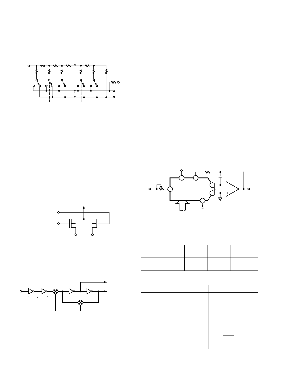
BASIC APPLICATIONS
Figures 4 and 5 show simple unipolar and bipolar circuits using
the AD7545. Resistor R1 is used to trim for full scale. The
“G” versions (AD7545GLN, AD7545GCQ, AD7545GUD)
have a guaranteed maximum gain error of
± 1 LSB at +25°C
(VDD = +5 V), and in many applications it should be possible to
dispense with gain trim resistors altogether. Capacitor C1 provides
phase compensation and helps prevent overshoot and ringing when
using high speed op amps. Note that all the circuits of Figures 4, 5
and 6 have constant input impedance at the VREF terminal.
The circuit of Figure 1 can either be used as a fixed reference
D/A converter so that it provides an analog output voltage in the
range 0 to –VIN (note the inversion introduced by the op amp),
or VIN can be an ac signal in which case the circuit behaves as
an attenuator (2-Quadrant Multiplier). VIN can be any voltage
in the range –20
≤ VIN + 20 volts (provided the op amp can
handle such voltages) since VREF is permitted to exceed VDD.
Table II shows the code relationship for the circuit of Figure 4.
VDD
R1
*
VIN
DB11–DB0
ANALOG
COMMON
R2
*
C1
33pF
AD544L
(SEE TEXT)
VOUT
*REFER TO TABLE I
20
18
1
2
3
19
AD7545
VDD
RFB
VREF
DGND
OUT1
AGND
Figure 4. Unipolar Binary Operation
Table I. Recommended Trim Resistor Values vs. Grades for
VDD = +5 V
Trim
Resistor
J/A/S
K/B/T
L/C/U
GL/GC/GU
R1
500
200
100
20
R2
150
68
33
6.8
Table II. Unipolar Binary Code Table for Circuit of Figure 4
Binary Number in DAC Register
Analog Output
1 1 1 1
–VIN
4095
4096
1 0 0 0
0 0 0 0
–VIN
2048
4096
= –1/2 VIN
0 0 0 0
0 0 0 1
–VIN
1
4096
0 0 0 0
0 Volts
相关PDF资料 |
PDF描述 |
|---|---|
| LTC1440CN8#PBF | IC COMP W/REF LP SINGLE 8-DIP |
| LTC491CS#PBF | IC TXRX RS485 LOW POWER 14-SOIC |
| AD7545ALN | IC DAC 12BIT W/BUFF MULT 20-DIP |
| VI-2NN-MX | CONVERTER MOD DC/DC 18.5V 75W |
| SY10EP89VZG | IC CABLE DRIVER COAXIAL 8-SOIC |
相关代理商/技术参数 |
参数描述 |
|---|---|
| AD7545KN/+ | 制造商:未知厂家 制造商全称:未知厂家 功能描述:12-Bit Digital-to-Analog Converter |
| AD7545KNZ | 功能描述:IC DAC 12BIT W/BUFF MULT 20-DIP RoHS:是 类别:集成电路 (IC) >> 数据采集 - 数模转换器 系列:- 产品培训模块:Data Converter Fundamentals DAC Architectures 标准包装:750 系列:- 设置时间:7µs 位数:16 数据接口:并联 转换器数目:1 电压电源:双 ± 功率耗散(最大):100mW 工作温度:0°C ~ 70°C 安装类型:表面贴装 封装/外壳:28-LCC(J 形引线) 供应商设备封装:28-PLCC(11.51x11.51) 包装:带卷 (TR) 输出数目和类型:1 电压,单极;1 电压,双极 采样率(每秒):143k |
| AD7545KP | 制造商:Rochester Electronics LLC 功能描述:- Bulk |
| AD7545LCWP | 制造商:未知厂家 制造商全称:未知厂家 功能描述:12-Bit Digital-to-Analog Converter |
| AD7545LD | 制造商:未知厂家 制造商全称:未知厂家 功能描述:Converter IC |
发布紧急采购,3分钟左右您将得到回复。