- 您现在的位置:买卖IC网 > PDF目录8595 > AD7564BR-REEL (Analog Devices Inc)IC DAC 12BIT QUAD 5V LP 28-SOIC PDF资料下载
参数资料
| 型号: | AD7564BR-REEL |
| 厂商: | Analog Devices Inc |
| 文件页数: | 6/17页 |
| 文件大小: | 0K |
| 描述: | IC DAC 12BIT QUAD 5V LP 28-SOIC |
| 产品培训模块: | Data Converter Fundamentals DAC Architectures |
| 标准包装: | 1,000 |
| 设置时间: | 500ns |
| 位数: | 12 |
| 数据接口: | 串行 |
| 转换器数目: | 4 |
| 电压电源: | 单电源 |
| 功率耗散(最大): | 50µW |
| 工作温度: | -40°C ~ 85°C |
| 安装类型: | 表面贴装 |
| 封装/外壳: | 28-SOIC(0.295",7.50mm 宽) |
| 供应商设备封装: | 28-SOIC W |
| 包装: | 带卷 (TR) |
| 输出数目和类型: | 8 电流,单极;8 电流,双极 |
| 采样率(每秒): | 1.8M |
REV.
AD7564
–14–
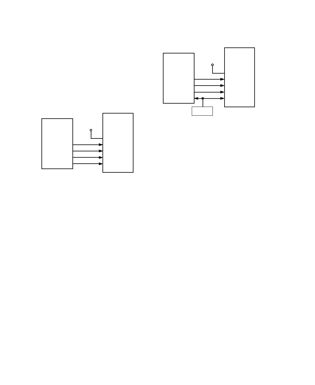
AD7564 to ADSP-2101/ADSP-2103 Interface
Figure 23 shows a serial interface between the AD7564 and the
ADSP-2101/ADSP-2103 digital signal processors. The ADSP-
2101 operates from 5 V while the ADSP-2103 operates from
3 V supplies. These processors are set up to operate in the
SPORT Transmit Alternate Framing Mode.
The following DSP conditions are recommended: Internal
SCLK; Active low Framing Signal; 16-bit word length. Trans-
mission is initiated by writing a word to the TX register after the
SPORT has been enabled. The data is then clocked out on ev-
ery rising edge of SCLK after TFS goes low. TFS stays low un-
til the next data transfer.
CLR
FSIN
SDIN
CLKIN
LDAC
TFS
DT
SCLK
FO
ADSP-2101/
ADSP-2103
AD7564*
*ADDITIONAL PINS OMMITTED FOR CLARITY
+5V
Figure 23. AD7564 to ADSP-2101/ADSP-2103 Interface
AD7564 to TMS320C25 Interface
Figure 24 shows an interface circuit for the TMS320C25 digital
signal processor. The data on the DX pin is clocked out of
the processor’s Transmit Shift Register by the CLKX signal.
Sixteen-bit transmit format should be chosen by setting the FO
bit in the ST1 register to 0. The transmit operation begins
when data is written into the data transmit register of the
TMS320C25. This data will be transmitted when the FSX line
goes low while CLKX is high or going high. The data, starting
with the MSB, is then shifted out to the DX pin on the rising
edge of CLKX. When all bits have been transmitted, the user
can update the DAC outputs by bringing the XF output flag
low.
CLR
FSIN
SDIN
CLKIN
LDAC
FSX
DX
CLKX
XF
TMS320C25*
AD7564*
*ADDITIONAL PINS OMMITTED FOR CLARITY
+5V
CLOCK
GENERATION
Figure 24. AD7564 to TMS320C25 Interface
APPLICATION HINTS
Output Offset
CMOS D/A converters in circuits such as Figures 17, 18 and 19
exhibit a code dependent output resistance which in turn can
cause a code dependent error voltage at the output of the ampli-
fier. The maximum amplitude of this error, which adds to the
D/A converter nonlinearity, depends on VOS, where VOS is the
amplifier input offset voltage. For the AD7564 to maintain
specified accuracy with VREF at 10 V, it is recommended that
VOS be no greater than 500 V, or (50 × 10
–6)
× (V
REF), over
the temperature range of operation. Suitable amplifiers include
the ADOP-07, ADOP-27, AD711, AD845 or multiple versions
of these.
Temperature Coefficients
The gain temperature coefficient of the AD7564 has a maxi-
mum value of 5 ppm/
°C and a typical value of 2 ppm/°C. This
corresponds to gain shifts of 2 LSBs and 0.8 LSBs respectively
over a 100
°C temperature range. When trim resistors R1 and
R2 are used to adjust full scale in Figures 17 and 18, their tem-
perature coefficients should be taken into account. For further
information see “Gain Error and Gain Temperature Coefficient
of CMOS Multiplying DACs,” Application Note, Publication
Number E630c-5-3/86, available from Analog Devices.
High Frequency Considerations
The output capacitances of the AD7564 DACs work in con-
junction with the amplifier feedback resistance to add a pole to
the open loop response. This can cause ringing or oscillation.
Stability can be restored by adding a phase compensation ca-
pacitor in parallel with the feedback resistor. This is shown as
C1 in Figures 17 and 18.
B
相关PDF资料 |
PDF描述 |
|---|---|
| SY88923KC | IC AMP POST 5V/3.3V 10-MSOP |
| VE-25T-IV-F3 | CONVERTER MOD DC/DC 6.5V 150W |
| VE-25R-IV-F3 | CONVERTER MOD DC/DC 7.5V 150W |
| SY88923AVKEC | IC AMP POST 5V/3.3V 10-MSOP |
| VE-23K-MY-B1 | CONVERTER MOD DC/DC 40V 50W |
相关代理商/技术参数 |
参数描述 |
|---|---|
| AD7564BRS | 功能描述:IC DAC 12BIT LC2MOS QUAD 28-SSOP RoHS:否 类别:集成电路 (IC) >> 数据采集 - 数模转换器 系列:- 产品培训模块:Data Converter Fundamentals DAC Architectures 标准包装:750 系列:- 设置时间:7µs 位数:16 数据接口:并联 转换器数目:1 电压电源:双 ± 功率耗散(最大):100mW 工作温度:0°C ~ 70°C 安装类型:表面贴装 封装/外壳:28-LCC(J 形引线) 供应商设备封装:28-PLCC(11.51x11.51) 包装:带卷 (TR) 输出数目和类型:1 电压,单极;1 电压,双极 采样率(每秒):143k |
| AD7564BRS-REEL | 功能描述:IC DAC 12BIT QUAD 5V LP 28-SSOP RoHS:否 类别:集成电路 (IC) >> 数据采集 - 数模转换器 系列:- 产品培训模块:Data Converter Fundamentals DAC Architectures 标准包装:750 系列:- 设置时间:7µs 位数:16 数据接口:并联 转换器数目:1 电压电源:双 ± 功率耗散(最大):100mW 工作温度:0°C ~ 70°C 安装类型:表面贴装 封装/外壳:28-LCC(J 形引线) 供应商设备封装:28-PLCC(11.51x11.51) 包装:带卷 (TR) 输出数目和类型:1 电压,单极;1 电压,双极 采样率(每秒):143k |
| AD7564BRSZ | 功能描述:IC DAC 12BIT 5V QUAD LP 28-SSOP RoHS:是 类别:集成电路 (IC) >> 数据采集 - 数模转换器 系列:- 产品培训模块:Lead (SnPb) Finish for COTS Obsolescence Mitigation Program 标准包装:50 系列:- 设置时间:4µs 位数:12 数据接口:串行 转换器数目:2 电压电源:单电源 功率耗散(最大):- 工作温度:-40°C ~ 85°C 安装类型:表面贴装 封装/外壳:8-TSSOP,8-MSOP(0.118",3.00mm 宽) 供应商设备封装:8-uMAX 包装:管件 输出数目和类型:2 电压,单极 采样率(每秒):* 产品目录页面:1398 (CN2011-ZH PDF) |
| AD7564BRSZ-REEL | 功能描述:IC DAC 12BIT QUAD 5V LP 28-SSOP RoHS:是 类别:集成电路 (IC) >> 数据采集 - 数模转换器 系列:- 产品培训模块:Data Converter Fundamentals DAC Architectures 标准包装:750 系列:- 设置时间:7µs 位数:16 数据接口:并联 转换器数目:1 电压电源:双 ± 功率耗散(最大):100mW 工作温度:0°C ~ 70°C 安装类型:表面贴装 封装/外壳:28-LCC(J 形引线) 供应商设备封装:28-PLCC(11.51x11.51) 包装:带卷 (TR) 输出数目和类型:1 电压,单极;1 电压,双极 采样率(每秒):143k |
| AD7564BRZ | 功能描述:IC DAC 12BIT LC2MOS QUAD 28-SOIC RoHS:是 类别:集成电路 (IC) >> 数据采集 - 数模转换器 系列:- 标准包装:1 系列:- 设置时间:4.5µs 位数:12 数据接口:串行,SPI? 转换器数目:1 电压电源:单电源 功率耗散(最大):- 工作温度:-40°C ~ 125°C 安装类型:表面贴装 封装/外壳:8-SOIC(0.154",3.90mm 宽) 供应商设备封装:8-SOICN 包装:剪切带 (CT) 输出数目和类型:1 电压,单极;1 电压,双极 采样率(每秒):* 其它名称:MCP4921T-E/SNCTMCP4921T-E/SNRCTMCP4921T-E/SNRCT-ND |
发布紧急采购,3分钟左右您将得到回复。