参数资料
| 型号: | AD7564BRS |
| 厂商: | Analog Devices Inc |
| 文件页数: | 5/17页 |
| 文件大小: | 0K |
| 描述: | IC DAC 12BIT LC2MOS QUAD 28-SSOP |
| 产品培训模块: | Data Converter Fundamentals DAC Architectures |
| 标准包装: | 1 |
| 设置时间: | 500ns |
| 位数: | 12 |
| 数据接口: | 串行 |
| 转换器数目: | 4 |
| 电压电源: | 单电源 |
| 功率耗散(最大): | 50µW |
| 工作温度: | -40°C ~ 85°C |
| 安装类型: | 表面贴装 |
| 封装/外壳: | 28-SSOP(0.209",5.30mm 宽) |
| 供应商设备封装: | 28-SSOP |
| 包装: | 管件 |
| 输出数目和类型: | 8 电流,单极;8 电流,双极 |
| 采样率(每秒): | 1.8M |
–13–
REV.
3
AD7564
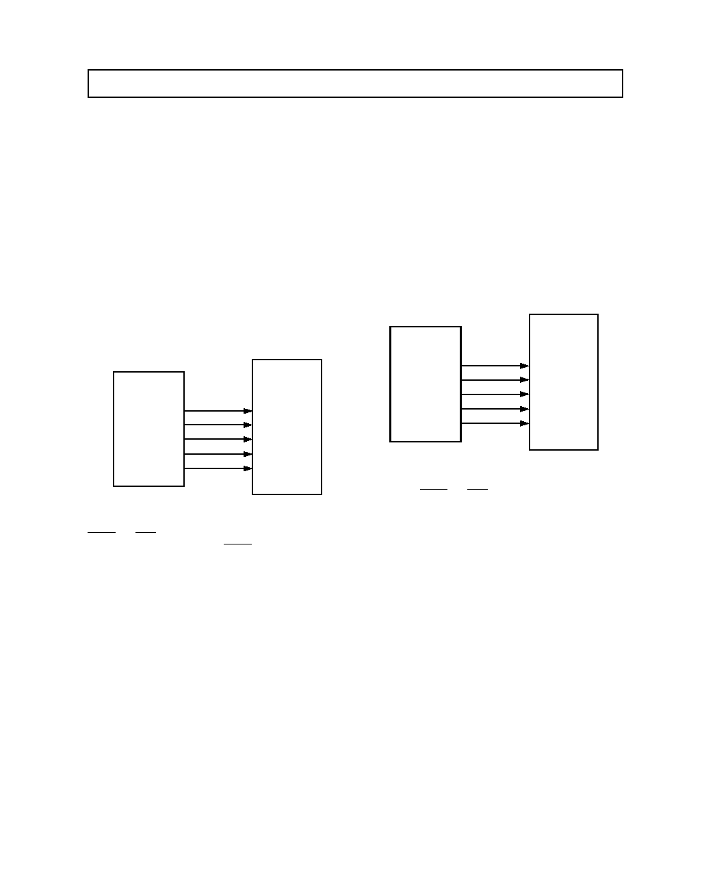
MICROPROCESSOR INTERFACING
AD7564 to 80C51 Interface
A serial interface between the AD7564 and the 80C51 micro-
controller is shown in Figure 21. TXD of the 80C51 drives
SCLK of the AD7564 while RXD drives the serial data line of
the part. The FSIN signal is derived from the port line P3.3.
The 80C51 provides the LSB of its SBUF register as the first bit
in the serial data stream. Therefore, the user will have to ensure
that the data in the SBUF register is arranged correctly so that
the data word transmitted to the AD7564 corresponds to the
loading sequence shown in Table I. When data is to be trans-
mitted to the part, P3.3 is taken low. Data on RXD is valid on
the falling edge of TXD. The 80C51 transmits its serial data in
8-bit bytes with only eight falling clock edges occurring in the
transmit cycle. To load data to the AD7564, P3.3 is left low
after the first eight bits are transferred and a second byte of data
is then transferred serially to the AD7564. When the second
serial transfer is complete, the P3.3 line is taken high. Note that
the 80C51 outputs the serial data byte in a format which has the
LSB first. The AD7564 expects the MSB first. The 80C51
transmit routine should take this into account.
CLR
FSIN
SCLK
SDIN
LDAC
P3.5
P3.3
TXD
RXD
P3.4
80C51*
AD7564*
*ADDITIONAL PINS OMMITTED FOR CLARITY
Figure 21. AD7564 to 80C51 Interface
LDAC
and CLR on the AD7564 are also controlled by 80C51
port outputs. The user can bring LDAC low after every two
bytes have been transmitted to update the DAC which has been
programmed. Alternatively, it is possible to wait until all the in-
put registers have been loaded (sixteen byte transmits) and then
update the DAC outputs.
AD7564 to 68HC11 Interface
Figure 22 shows a serial interface between the AD7564 and the
68HC11 microcontroller. SCK of the 68HC11 drives SCLK of
the AD7564 while the MOSI output drives the serial data line of
the AD7564. The FSIN signal is derived from a port line
(PC7 shown).
For correct operation of this interface, the 68HC11 should be
configured such that its CPOL bit is a 0 and its CPHA bit is a 1.
When data is to be transmitted to the part, PC7 is taken low.
When the 68HC11 is configured like this, data on MOSI is valid
on the falling edge of SCK. The 68HC11 transmits its serial
data in 8-bit bytes (MSB first), with only eight falling clock
edges occurring in the transmit cycle. To load data to the
AD7564 , PC7 is left low after the first eight bits are transferred
and a second byte of data is then transferred serially to the
AD7564. When the second serial transfer is complete, the PC7
line is taken high.
CLR
FSIN
SCLK
SDIN
LDAC
PC5
PC7
SCK
MOSI
PC6
64HC11*
AD7564*
*ADDITIONAL PINS OMMITTED FOR CLARITY
Figure 22. AD7564 to 64HC11 Interface
In Figure 22, LDAC and CLR are controlled by the PC6
and PC5 port outputs. As with the 80C51, each DAC of the
AD7564 can be updated after each two-byte transfer, or else
all DACs can be simultaneously updated. This interface
is suitable for both 3 V and 5 V versions of the 68HC11
microcontroller.
B
相关PDF资料 |
PDF描述 |
|---|---|
| AD766JN | IC DAC 16BIT W/VREF 16-DIP |
| VE-26Y-MY-B1 | CONVERTER MOD DC/DC 3.3V 33W |
| VE-26Y-MX-B1 | CONVERTER MOD DC/DC 3.3V 49.5W |
| VE-26X-MY-B1 | CONVERTER MOD DC/DC 5.2V 50W |
| VE-26W-MY-B1 | CONVERTER MOD DC/DC 5.5V 50W |
相关代理商/技术参数 |
参数描述 |
|---|---|
| AD7564BRS-REEL | 功能描述:IC DAC 12BIT QUAD 5V LP 28-SSOP RoHS:否 类别:集成电路 (IC) >> 数据采集 - 数模转换器 系列:- 产品培训模块:Data Converter Fundamentals DAC Architectures 标准包装:750 系列:- 设置时间:7µs 位数:16 数据接口:并联 转换器数目:1 电压电源:双 ± 功率耗散(最大):100mW 工作温度:0°C ~ 70°C 安装类型:表面贴装 封装/外壳:28-LCC(J 形引线) 供应商设备封装:28-PLCC(11.51x11.51) 包装:带卷 (TR) 输出数目和类型:1 电压,单极;1 电压,双极 采样率(每秒):143k |
| AD7564BRSZ | 功能描述:IC DAC 12BIT 5V QUAD LP 28-SSOP RoHS:是 类别:集成电路 (IC) >> 数据采集 - 数模转换器 系列:- 产品培训模块:Lead (SnPb) Finish for COTS Obsolescence Mitigation Program 标准包装:50 系列:- 设置时间:4µs 位数:12 数据接口:串行 转换器数目:2 电压电源:单电源 功率耗散(最大):- 工作温度:-40°C ~ 85°C 安装类型:表面贴装 封装/外壳:8-TSSOP,8-MSOP(0.118",3.00mm 宽) 供应商设备封装:8-uMAX 包装:管件 输出数目和类型:2 电压,单极 采样率(每秒):* 产品目录页面:1398 (CN2011-ZH PDF) |
| AD7564BRSZ-REEL | 功能描述:IC DAC 12BIT QUAD 5V LP 28-SSOP RoHS:是 类别:集成电路 (IC) >> 数据采集 - 数模转换器 系列:- 产品培训模块:Data Converter Fundamentals DAC Architectures 标准包装:750 系列:- 设置时间:7µs 位数:16 数据接口:并联 转换器数目:1 电压电源:双 ± 功率耗散(最大):100mW 工作温度:0°C ~ 70°C 安装类型:表面贴装 封装/外壳:28-LCC(J 形引线) 供应商设备封装:28-PLCC(11.51x11.51) 包装:带卷 (TR) 输出数目和类型:1 电压,单极;1 电压,双极 采样率(每秒):143k |
| AD7564BRZ | 功能描述:IC DAC 12BIT LC2MOS QUAD 28-SOIC RoHS:是 类别:集成电路 (IC) >> 数据采集 - 数模转换器 系列:- 标准包装:1 系列:- 设置时间:4.5µs 位数:12 数据接口:串行,SPI? 转换器数目:1 电压电源:单电源 功率耗散(最大):- 工作温度:-40°C ~ 125°C 安装类型:表面贴装 封装/外壳:8-SOIC(0.154",3.90mm 宽) 供应商设备封装:8-SOICN 包装:剪切带 (CT) 输出数目和类型:1 电压,单极;1 电压,双极 采样率(每秒):* 其它名称:MCP4921T-E/SNCTMCP4921T-E/SNRCTMCP4921T-E/SNRCT-ND |
| AD7564BRZ-REEL | 功能描述:IC DAC 12BIT QUAD 5V LP 28SOIC RoHS:是 类别:集成电路 (IC) >> 数据采集 - 数模转换器 系列:- 产品培训模块:Data Converter Fundamentals DAC Architectures 标准包装:750 系列:- 设置时间:7µs 位数:16 数据接口:并联 转换器数目:1 电压电源:双 ± 功率耗散(最大):100mW 工作温度:0°C ~ 70°C 安装类型:表面贴装 封装/外壳:28-LCC(J 形引线) 供应商设备封装:28-PLCC(11.51x11.51) 包装:带卷 (TR) 输出数目和类型:1 电压,单极;1 电压,双极 采样率(每秒):143k |
发布紧急采购,3分钟左右您将得到回复。