- 您现在的位置:买卖IC网 > PDF目录11767 > AD7569BRZ (Analog Devices Inc)IC I/O PORT 8BIT ANALOG 24SOIC PDF资料下载
参数资料
| 型号: | AD7569BRZ |
| 厂商: | Analog Devices Inc |
| 文件页数: | 7/20页 |
| 文件大小: | 0K |
| 描述: | IC I/O PORT 8BIT ANALOG 24SOIC |
| 标准包装: | 31 |
| 系列: | LC²MOS |
| 应用: | 模拟 I/O |
| 接口: | 总线 |
| 电源电压: | 4.75 V ~ 5.25 V |
| 封装/外壳: | 24-SOIC(0.295",7.50mm 宽) |
| 供应商设备封装: | 24-SOIC W |
| 包装: | 管件 |
| 安装类型: | 表面贴装 |
AD7569/AD7669
–15–
REV. B
an RD pulse for the AD7569/AD7669. This RD pulse accesses
data from the ADC and places the conversion result into a regis-
ter on the 74646. The rising edge of this pulse generates an in-
terrupt request to the processor. The conversion result is read
from the 74646 register by performing an I/O read to the
decoded address of the 74646. Writing data to the relevant
AD7569/AD7669 DAC involves an I/O write to the 74646,
which transfers the data to the data inputs of the AD7569/
AD7669. Data is latched into the selected DAC register on the
rising edge of IOW.
APPLYING THE AD7569/AD7669 DAC
An internal gain/offset network on the AD7569/AD7669 allows
several output voltage ranges. The part can produce unipolar
output ranges of 0 V to +1.25 V or 0 V to +2.5 V and bipolar
output ranges of –1.25 V to +1.25 V or –2.5 V to +2.5 V. Con-
nections for these various output ranges are outlined below.
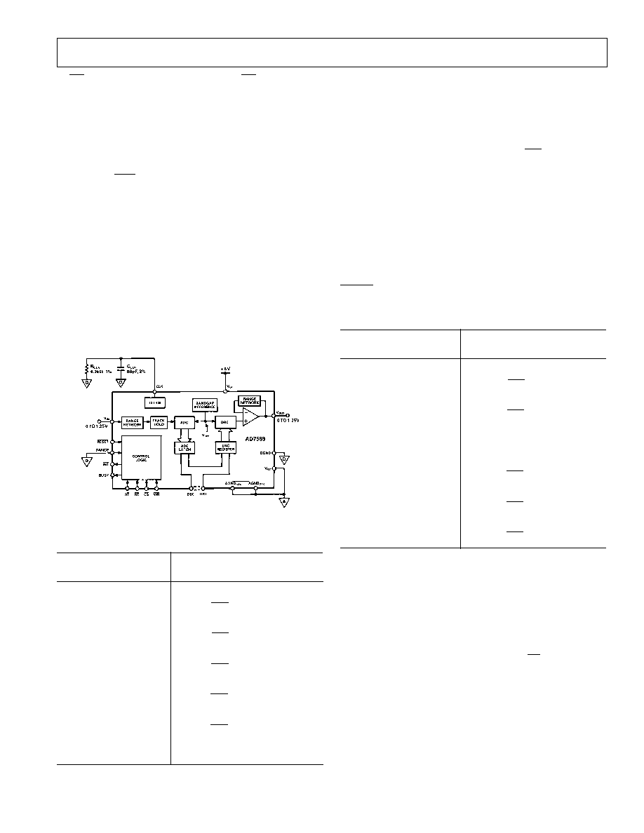
UNIPOLAR (0 V to +1.25 V) CONFIGURATION
The first of the configurations provides an output voltage range
of 0 V to +1.25 V. This is achieved by tying the VSS and
RANGE inputs to AGNDDAC(= 0 V). Figure 21 shows the con-
figuration of the AD7569 to achieve this output range. A similar
configuration of the AD7669 gives the same output range. The
table for output voltage versus the digital code in the DAC regis-
ter is shown in Table IV.
Figure 21. AD7569 Unipolar (0 V to +1.25 V) Operation
Table IV. Unipolar (0 V to +1.25 V) Code Table
DAC Register Contents
MSB
LSB
Analog Output, VOUT
1111
+VREF
255
256
1000
0001
+VREF
129
256
1000
0000
+VREF
128
256
= +VREF/2
0111
1111
+VREF
127
256
0000
0001
+VREF
1
256
0000
0 V
NOTE: 1 LSB = (VREF) (2
–8) = V
REF (1/256); VREF = +1.25 V Nominal
UNIPOLAR (0 V to +2.5 V) CONFIGURATION
The 0 V to +2.5 V output voltage range is achieved by tying VSS
to AGNDDAC(= 0 V) and the RANGE input to VDD. The table
for output voltage versus digital code is as in Table IV with
2.VREF replacing VREF. Note that for this range
1 LSB
= 2.V
REF (2
8 ) = V
REF
1
128
BIPOLAR (–1.25 V to +1.25 V) CONFIGURATION
The first of the bipolar configurations is achieved by tying the
RANGE input to AGNDDAC(= 0 V) and VSS to –5 V. The VSS
voltage level at which the AD7569/AD7669 changes to bipolar
operation is approximately –1 V. When the part is configured
for bipolar outputs, the input coding becomes twos comple-
ment. The table for output voltage versus the digital code in the
DAC register is shown in Table V. Note as with the unipolar
configuration, a digital input code of all 0s produces an output
of 0 V. It should be noted, however, that a low pulse on the
RESET
line for the bipolar ranges sets the output voltage to
negative full scale.
Table V. Bipolar (–1.25 V to +1.25 V) Code Table
DAC Register Contents
MSB
LSB
Analog Output, VOUT
0111
1111
+VREF
127
128
0000
0001
+VREF
1
128
0000
0 V
1111
–VREF
1
128
1000
0001
–VREF
127
128
1000
0000
–VREF
128
= –VREF
NOTE: 1 LSB = (VREF)(2
–7) = V
REF (1/128)
BIPOLAR (–2.5 V to +2.5 V) CONFIGURATION
The –2.5 V to +2.5 V bipolar output range is achieved by tying
the RANGE input to VDD and the VSS input to –5 V. Once
again, the input coding is 2s complement. The table for output
voltage versus digital code is as in Table V with 2.VREF replacing
VREF. Note that for this range
1 LSB
= 4.V
REF (2
8 ) = V
REF
1
64
相关PDF资料 |
PDF描述 |
|---|---|
| PIC16F723A-I/SP | MCU PIC 7KB FLASH XLP 28-SPDIP |
| PIC16C505-04/SL | IC MCU OTP 1KX12 14SOIC |
| PIC16LF1825-I/P | MCU PIC 14KB FLASH 14-DIP |
| PIC16LF1826-I/MV | IC MCU 8BIT FLASH 28UQFN |
| AD7669AR | IC I/O PORT 8BIT ANLG 28-SOIC |
相关代理商/技术参数 |
参数描述 |
|---|---|
| AD7569JN | 功能描述:IC I/O PORT 8BIT ANLG 24-DIP RoHS:否 类别:集成电路 (IC) >> 接口 - 专用 系列:LC²MOS 标准包装:3,000 系列:- 应用:PDA,便携式音频/视频,智能电话 接口:I²C,2 线串口 电源电压:1.65 V ~ 3.6 V 封装/外壳:24-WQFN 裸露焊盘 供应商设备封装:24-QFN 裸露焊盘(4x4) 包装:带卷 (TR) 安装类型:表面贴装 产品目录页面:1015 (CN2011-ZH PDF) 其它名称:296-25223-2 |
| AD7569JNZ | 功能描述:IC I/O PORT 8BIT ANALOG 24DIP RoHS:是 类别:集成电路 (IC) >> 接口 - 专用 系列:LC²MOS 特色产品:NXP - I2C Interface 标准包装:1 系列:- 应用:2 通道 I²C 多路复用器 接口:I²C,SM 总线 电源电压:2.3 V ~ 5.5 V 封装/外壳:16-TSSOP(0.173",4.40mm 宽) 供应商设备封装:16-TSSOP 包装:剪切带 (CT) 安装类型:表面贴装 产品目录页面:825 (CN2011-ZH PDF) 其它名称:568-1854-1 |
| AD7569JP | 功能描述:IC I/O PORT 8BIT ANLG 28-PLCC RoHS:否 类别:集成电路 (IC) >> 接口 - 专用 系列:LC²MOS 特色产品:NXP - I2C Interface 标准包装:1 系列:- 应用:2 通道 I²C 多路复用器 接口:I²C,SM 总线 电源电压:2.3 V ~ 5.5 V 封装/外壳:16-TSSOP(0.173",4.40mm 宽) 供应商设备封装:16-TSSOP 包装:剪切带 (CT) 安装类型:表面贴装 产品目录页面:825 (CN2011-ZH PDF) 其它名称:568-1854-1 |
| ad7569jp-reel | 制造商:Rochester Electronics LLC 功能描述: 制造商:Analog Devices 功能描述: |
| AD7569JPZ | 功能描述:IC I/O PORT 8BIT ANLG 28PLCC RoHS:是 类别:集成电路 (IC) >> 接口 - 专用 系列:LC²MOS 特色产品:NXP - I2C Interface 标准包装:1 系列:- 应用:2 通道 I²C 多路复用器 接口:I²C,SM 总线 电源电压:2.3 V ~ 5.5 V 封装/外壳:16-TSSOP(0.173",4.40mm 宽) 供应商设备封装:16-TSSOP 包装:剪切带 (CT) 安装类型:表面贴装 产品目录页面:825 (CN2011-ZH PDF) 其它名称:568-1854-1 |
发布紧急采购,3分钟左右您将得到回复。