- 您现在的位置:买卖IC网 > PDF目录373909 > AD7575AQ (ANALOG DEVICES INC) LC2MOS 5 us 8-Bit ADC with Track/Hold PDF资料下载
参数资料
| 型号: | AD7575AQ |
| 厂商: | ANALOG DEVICES INC |
| 元件分类: | ADC |
| 英文描述: | LC2MOS 5 us 8-Bit ADC with Track/Hold |
| 中文描述: | 1-CH 8-BIT SUCCESSIVE APPROXIMATION ADC, PARALLEL ACCESS, CDIP18 |
| 封装: | 0.300 INCH, CERDIP-18 |
| 文件页数: | 6/12页 |
| 文件大小: | 146K |
| 代理商: | AD7575AQ |
AD7575
–6–
REV. B
AD7575*
TP
CS
RD
DB0–DB7
ADDRESS BUS
DATA BUS
+5V
*LINEAR CIRCUITRY OMITTED FOR CLARITY
ADDRESS
DECODE
EN
A0–A15
R/
W
f
2 OR E
D0–D7
6502/6809
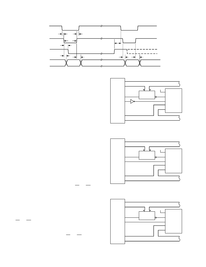
Figure 6. AD7575 to 6502/6809 ROM Interface
AD7575*
TP
CS
RD
ADDRESS BUS
DATA BUS
+5V
*LINEAR CIRCUITRY OMITTED FOR CLARITY
ADDRESS
DECODE
EN
MREQ
Z–80
RD
DB7
DB0
DB7
DB0
Figure 7. AD7575 to Z-80 ROM Interface
AD7575*
TP
CS
RD
ADDRESS BUS
DATA BUS
+5V
*LINEAR CIRCUITRY OMITTED FOR CLARITY
ADDRESS
DECODE
EN
MEN
TMS32010
DEN
D7
D0
DB7
DB0
PA2
PA0
Figure 8. AD7575 to TMS32010 ROM Interface
Figures 6 and 7 show connection diagrams for interfacing the
AD7575 in the ROM Interface mode. Figure 6 shows the
AD7575 interface to the 6502/6809 microprocessors while the
connection diagram for interfacing to the Z-80 is shown in
Figure 7.
As a result of its very fast interface timing, the AD7575 can also
be interfaced to the DSP processor, the TMS32010. The
AD7575 will (within specifications) interface to the TMS32010,
running at up to 18 MHz, but will typically work over the full
clock frequency range of the TMS32010. Figure 8 shows the
connection diagram for this interface. The AD7575 is mapped
at a port address. Conversion is initiated using an IN A, PA
instruction where PA is the decoded port address for the
AD7575. The conversion result is obtained from the part using
a second IN A, PA instruction, and the resultant data is placed
in the TMS32010 accumulator.
In many applications it is important that the signal sampling
occurs at exactly equal intervals to minimize errors due to sam-
pling uncertainty or jitter. The interfaces outlined previously
require that for sampling at equidistant intervals, the user must
count clock cycles or match software delays. This is especially
difficult in interrupt-driven systems where uncertainty in inter-
rupt servicing delays would require that the AD7575 have prior-
ity interrupt status and even then redundant software delays
may be necessary to equalize loop delays.
This problem can be overcome by using a real time clock to
control the starting of conversion. This can be derived from the
clock source used to drive the AD7575 CLK pin. Since the
sampling instant occurs three clock cycles after
CS
and
RD
go
LOW, the input signal sampling intervals are equidistant. The
resultant data is placed in a FIFO latch that can be accessed by
the microprocessor at its own rate whenever it requires the data.
This ensures that data is not READ from the AD7575 during a
conversion. If a data READ is performed during a conversion,
valid data from the previous conversion will be accessed, but the
conversion in progress may be interfered with and an incorrect
result is likely.
If
CS
and
RD
go LOW within 20 ns of a falling clock edge, the
AD7575 may or may not see that falling edge as the first of the
three falling clock edges to the sampling instant. In this case, the
sampling instant could vary by one clock period. If it is impor-
tant to know the exact sampling instant,
CS
and
RD
should not
go LOW within 20 ns of a falling clock edge.
HIGH IMPEDANCE
BUS
NEW
DATA
HIGH
IMPEDANCE BUS
HIGH IMPEDANCE
BUS
OLD
DATA
DATA
BUSY
RD
CS
t
1
t
2
t
3
t
5
t
7
t
8
t
4
t
7
t
3
Figure 5. ROM Interface Timing Diagram
相关PDF资料 |
PDF描述 |
|---|---|
| AD7575BQ | LC2MOS 5 us 8-Bit ADC with Track/Hold |
| AD7575JN | LC2MOS 5 us 8-Bit ADC with Track/Hold |
| AD7575JP | LC2MOS 5 us 8-Bit ADC with Track/Hold |
| AD7575JR | LC2MOS 5 us 8-Bit ADC with Track/Hold |
| AD7575KN | LC2MOS 5 us 8-Bit ADC with Track/Hold |
相关代理商/技术参数 |
参数描述 |
|---|---|
| AD7575BQ | 功能描述:IC ADC 8BIT LC2MOS W/HOLD 18CDIP RoHS:否 类别:集成电路 (IC) >> 数据采集 - 模数转换器 系列:- 标准包装:1,000 系列:- 位数:12 采样率(每秒):300k 数据接口:并联 转换器数目:1 功率耗散(最大):75mW 电压电源:单电源 工作温度:0°C ~ 70°C 安装类型:表面贴装 封装/外壳:24-SOIC(0.295",7.50mm 宽) 供应商设备封装:24-SOIC 包装:带卷 (TR) 输入数目和类型:1 个单端,单极;1 个单端,双极 |
| AD7575JN | 功能描述:IC ADC 8BIT LC2MOS W/HOLD 18-DIP RoHS:否 类别:集成电路 (IC) >> 数据采集 - 模数转换器 系列:- 产品培训模块:Lead (SnPb) Finish for COTS Obsolescence Mitigation Program 标准包装:2,500 系列:- 位数:12 采样率(每秒):3M 数据接口:- 转换器数目:- 功率耗散(最大):- 电压电源:- 工作温度:- 安装类型:表面贴装 封装/外壳:SOT-23-6 供应商设备封装:SOT-23-6 包装:带卷 (TR) 输入数目和类型:- |
| AD7575JNZ | 功能描述:IC ADC 8BIT LC2MOS W/HOLD 18DIP RoHS:是 类别:集成电路 (IC) >> 数据采集 - 模数转换器 系列:- 标准包装:1,000 系列:- 位数:12 采样率(每秒):300k 数据接口:并联 转换器数目:1 功率耗散(最大):75mW 电压电源:单电源 工作温度:0°C ~ 70°C 安装类型:表面贴装 封装/外壳:24-SOIC(0.295",7.50mm 宽) 供应商设备封装:24-SOIC 包装:带卷 (TR) 输入数目和类型:1 个单端,单极;1 个单端,双极 |
| AD7575JP | 制造商:Analog Devices 功能描述:ADC Single SAR 8-bit Parallel 20-Pin PLCC 制造商:Rochester Electronics LLC 功能描述:CMOS CONVERTER IC - Bulk |
| AD7575JP-REEL | 制造商:Analog Devices 功能描述:ADC Single SAR 8-bit Parallel 20-Pin PLCC T/R |
发布紧急采购,3分钟左右您将得到回复。