- 您现在的位置:买卖IC网 > PDF目录10247 > AD7575JRZ (Analog Devices Inc)IC ADC 8BIT LC2MOS W/HOLD 18SOIC PDF资料下载
参数资料
| 型号: | AD7575JRZ |
| 厂商: | Analog Devices Inc |
| 文件页数: | 12/12页 |
| 文件大小: | 0K |
| 描述: | IC ADC 8BIT LC2MOS W/HOLD 18SOIC |
| 标准包装: | 41 |
| 位数: | 8 |
| 采样率(每秒): | 50k |
| 数据接口: | 并联 |
| 转换器数目: | 1 |
| 功率耗散(最大): | 15mW |
| 电压电源: | 单电源 |
| 工作温度: | 0°C ~ 70°C |
| 安装类型: | 表面贴装 |
| 封装/外壳: | 18-SOIC(0.295",7.50mm 宽) |
| 供应商设备封装: | 18-SOIC |
| 包装: | 管件 |
| 输入数目和类型: | 1 个单端,单极;1 个单端,双极 |
AD7575
–9–
REV. B
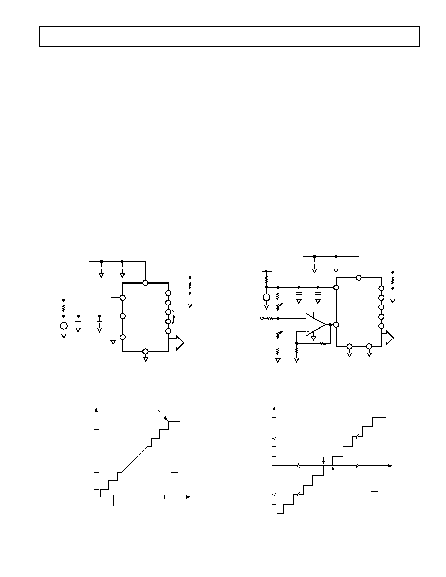
UNIPOLAR OPERATION
The basic operation for the AD7575 is in the unipolar single
supply mode. Figure 15 shows the circuit connections to achieve
this, while the nominal transfer characteristic for unipolar opera-
tion is given in Figure 16. Since the offset and full-scale errors
on the AD7575 are very small, in many cases it will not be nec-
essary to adjust out these errors. If calibration is required, the
procedure is as follows:
Offset Adjust
Offset error adjustment in single-supply systems is easily achiev-
able by means of the offset null facility of an op amp when used
as a voltage follower for the analog input signal, AIN. The op
amp chosen should be able to operate from a single supply and
allow a common-mode input voltage range that includes 0 V
(e.g., TLC271). To adjust for zero offset, the input signal
source is set to +4.8 mV (i.e., 1/2 LSB) while the op amp offset
is varied until the ADC output code flickers between 000 . . . 00
and 000 . . . 01.
Full-Scale Adjust
The full scale or gain adjustment is made by forcing the analog
input AIN to +2.445 V (i.e., Full-Scale Voltage –3/2 LSB). The
magnitude of the reference voltage is then adjusted until the
ADC output code flickers between 111 . . . 10 and 111. . . 11.
BIPOLAR OPERATION
The circuit of Figure 17 shows how the AD7575 can be config-
ured for bipolar operation. The output code provided by the
AD7575 is offset binary. The analog input voltage range is
±5 V, although the voltage appearing at the AIN pin of the
AD7575 is in the range 0 V to +2.46 V. Figure 18 shows the
transfer function for bipolar operation. The LSB size is now
39.06 mV. Calibration of the bipolar operation is outlined be-
low. Once again, because the errors are small, it may not be
necessary to adjust them. To maintain specified performance
without the calibration, all resistors should be 0.1% tolerance
with R4 and R5 replaced by one 3.3 k
resistor and R2 and R3
replaced by one 2.5 k
resistor.
Offset Adjust
Offset error adjustment is achieved by applying an analog input
voltage of –4.9805 V (–FS +1/2 LSB). Resistor R3 is then
adjusted until the output code flickers between 000 . . . 00 and
000 . . . 01.
Full-Scale Adjust
Full-scale or gain adjustment is made by applying an analog
input voltage of +4.9414 V (+FS –3/2 LSB). Resistor R4 is then
adjusted until the output code flickers between 111 . . . 10 and
111. . . 11.
A
47 F
0.1 F
+5V
+2.46V
MAX
A
47 F
0.1 F
A
+
–
AD589
3.3k
+5V
+1.23V
CONTROL
INPUTS
+5V
AIN
VREF
AGND
CLK
BUSY
CS
RD
TP
VDD
D
DB7–DB0
DATA OUT
AD7575
DGND
D
+5V
RCLK
100k , 1%
CCLK
100pF, 2%
Figure 15. Unipolar Configuration
OUTPUT
CODE
FULL SCALE
TRANSITION
11111111
11111110
11111101
00000011
00000010
00000001
00000000
FS = 2VREF
1LSB =
FS
256
1LSB
3LSBs
2LSBs
FS
FS –1LSB
AIN, INPUT VOLTAGE (IN TERMS OF LSBs)
Figure 16. Nominal Transfer Characteristic for
Unipolar Operation
A
47 F
0.1 F
+5V
A
47 F
0.1 F
A
+
–
AD589
+5V
AIN
VREF
CLK
BUSY
CS
RD
TP
VDD
D
DB7–DB0
DATA OUT
AD7575
DGND
D
+5V
RCLK
100k , 1%
CCLK
100pF, 2%
+
A
AGND
R2
2.2k
R3
500
INPUT
VOLTAGE
R4
500
R5
3k
A
+5V
R7
2.5k
R6
2.5k
A
TLC271
R8
3.3k
R1
10k
Figure 17. Bipolar Configuration
–1/2LSB
+1/2LSB
–FS
+FS –1LSB
AIN
FS = 5V
1LSB =
FS
256
OUTPUT
CODE
111...111
111...110
100...010
100...001
100...000
011...111
011...110
000...001
000...000
Figure 18. Nominal Transfer Characteristic for
Bipolar Operation
相关PDF资料 |
PDF描述 |
|---|---|
| VE-23Y-MV-F3 | CONVERTER MOD DC/DC 3.3V 99W |
| VE-23H-CU-F4 | CONVERTER MOD DC/DC 52V 200W |
| AD7988-5BRMZ-RL7 | IC ADC 16BIT SRL 500KSPS 10MSOP |
| VE-23H-CU-F3 | CONVERTER MOD DC/DC 52V 200W |
| LTC1418IN#PBF | IC A/D CONV 14BIT SRL&PAR 28-DIP |
相关代理商/技术参数 |
参数描述 |
|---|---|
| AD7575KN | 制造商:Rochester Electronics LLC 功能描述:CMOS CONVERTER IC - Bulk 制造商:Analog Devices 功能描述: |
| AD7575KNZ | 功能描述:IC ADC 8BIT LC2MOS W/HOLD 18DIP RoHS:是 类别:集成电路 (IC) >> 数据采集 - 模数转换器 系列:- 标准包装:1,000 系列:- 位数:12 采样率(每秒):300k 数据接口:并联 转换器数目:1 功率耗散(最大):75mW 电压电源:单电源 工作温度:0°C ~ 70°C 安装类型:表面贴装 封装/外壳:24-SOIC(0.295",7.50mm 宽) 供应商设备封装:24-SOIC 包装:带卷 (TR) 输入数目和类型:1 个单端,单极;1 个单端,双极 |
| AD7575KP | 制造商:Rochester Electronics LLC 功能描述:CMOS CONVERTER IC - Bulk |
| AD7575KP-REEL | 制造商:Analog Devices 功能描述:ADC Single SAR 8-bit Parallel 20-Pin PLCC T/R 制造商:Analog Devices 功能描述:ADC SGL SAR 8BIT PARALLEL 20PLCC - Tape and Reel 制造商:Rochester Electronics LLC 功能描述:8-BIT ADC WITH T/H IC - Tape and Reel |
| AD7575KPZ | 功能描述:IC ADC 8BIT LC2MOS W/HOLD 20PLCC RoHS:是 类别:集成电路 (IC) >> 数据采集 - 模数转换器 系列:- 标准包装:1,000 系列:- 位数:12 采样率(每秒):300k 数据接口:并联 转换器数目:1 功率耗散(最大):75mW 电压电源:单电源 工作温度:0°C ~ 70°C 安装类型:表面贴装 封装/外壳:24-SOIC(0.295",7.50mm 宽) 供应商设备封装:24-SOIC 包装:带卷 (TR) 输入数目和类型:1 个单端,单极;1 个单端,双极 |
发布紧急采购,3分钟左右您将得到回复。