- 您现在的位置:买卖IC网 > PDF目录10197 > AD7575KPZ (Analog Devices Inc)IC ADC 8BIT LC2MOS W/HOLD 20PLCC PDF资料下载
参数资料
| 型号: | AD7575KPZ |
| 厂商: | Analog Devices Inc |
| 文件页数: | 8/12页 |
| 文件大小: | 0K |
| 描述: | IC ADC 8BIT LC2MOS W/HOLD 20PLCC |
| 标准包装: | 49 |
| 位数: | 8 |
| 采样率(每秒): | 50k |
| 数据接口: | 并联 |
| 转换器数目: | 1 |
| 功率耗散(最大): | 15mW |
| 电压电源: | 单电源 |
| 工作温度: | 0°C ~ 70°C |
| 安装类型: | 表面贴装 |
| 封装/外壳: | 20-LCC(J 形引线) |
| 供应商设备封装: | 20-PLCC(9x9) |
| 包装: | 管件 |
| 输入数目和类型: | 1 个单端,单极;1 个单端,双极 |
AD7575
–5–
REV. B
TIMING AND CONTROL OF THE AD7575
The two logic inputs on the AD7575,
CS and RD, control both
the starting of conversion and the reading of data from the part.
A conversion is initiated by bringing both of these control inputs
LOW. Two interface options then exist for reading the output
data from the AD7575. These are the Slow Memory Interface
and ROM Interface, their operation is outlined below. It should
be noted that the TP pin of the AD7575 must be hard-wired
HIGH to ensure correct operation of the part. This pin is used
in testing the device and should not be used as a feedthrough pin
in double-sided printed circuit boards.
SLOW MEMORY INTERFACE
The first interface option is intended for use with microproces-
sors that can be forced into a WAIT STATE for at least 5
s.
The microprocessor (such as the 8085A) starts a conversion and
is halted until the result of the conversion is read from the con-
verter. Conversion is initiated by executing a memory READ to
the AD7575 address, bringing
CS and RD LOW. BUSY subse-
quently goes LOW (forcing the microprocessor READY input
LOW), placing the processor into a WAIT state. The input
signal, which had been tracked by the analog input, is held on
the third falling clock edge of the input clock after
CS and RD
have gone LOW (see Figure 12). The AD7575 then performs a
conversion on this acquired input signal value. When the con-
version is complete (
BUSY goes HIGH), the processor com-
pletes the memory READ and acquires the newly converted
data. The timing diagram for this interface is shown in Figure 3.
ADDRESS
DECODE
ADDRESS
LATCH
AD7575*
TP
CS
RD
BUSY
DB0–DB7
ADDRESS BUS
DATA BUS
+5V
A8–A15
S0
ALE
AD0–AD7
READY
8085A–2
*LINEAR CIRCUITRY OMITTED FOR CLARITY
SO = 0 FOR READ CYCLES
Figure 4. AD7575 to 8085A-2 Slow Memory Interface
The major advantage of this interface is that it allows the micro-
processor to start conversion, WAIT, and then READ data with
a single READ instruction. The fast conversion time of the
AD7575 ensures that the microprocessor is not placed in a
WAIT state for an excessive amount of time.
Faster versions of many processors, including the 8085A-2, test
the condition of the READY input very soon after the start of
an instruction cycle. Therefore,
BUSY of the AD7575 must go
LOW very early in the cycle for the READY input to be effec-
tive in forcing the processor into a WAIT state. When using the
8085A-2, the processor S0 status signal provides the earliest
possible indication that a READ operation is about to occur.
Hence, S0 (which is LOW for a READ cycle) provides the
READ signal to the AD7575. The connection diagram for the
AD7575 to 8085A-2 Slow Memory interface is shown in
Figure 4.
ROM INTERFACE
The alternative interface option on the AD7575 avoids placing
the microprocessor into a WAIT state. In this interface, a con-
version is started with the first READ instruction, and the sec-
ond READ instruction accesses the data and starts a second
conversion. The timing diagram for this interface is shown in
Figure 5. It is possible to avoid starting another conversion on
the second READ (see below).
Conversion is initiated by executing a memory READ instruc-
tion to the AD7575 address, causing
CS and RD to go LOW.
Data is also obtained from the AD7575 during this instruction.
This is old data and may be disregarded if not required.
BUSY
goes LOW, indicating that conversion is in progress, and re-
turns HIGH when conversion is complete. Once again, the
input signal is held on the third falling edge of the input clock
after
CS and RD have gone LOW.
The
BUSY line may be used to generate an interrupt to the
microprocessor or monitored to indicate that conversion is
complete. The processor then reads the newly-converted data.
Alternatively, the delay between the convert start (first READ
instruction) and the data READ (second READ instruction)
must be at least as great as the AD7575 conversion time. For
the AD7575 to operate correctly in the ROM interface mode,
CS and RD should not go LOW before BUSY returns HIGH.
Normally, the second READ instruction starts another conver-
sion as well as accessing the output data. However, if
CS and
RD are brought LOW within one external clock period of
BUSY going HIGH, a second conversion does not occur.
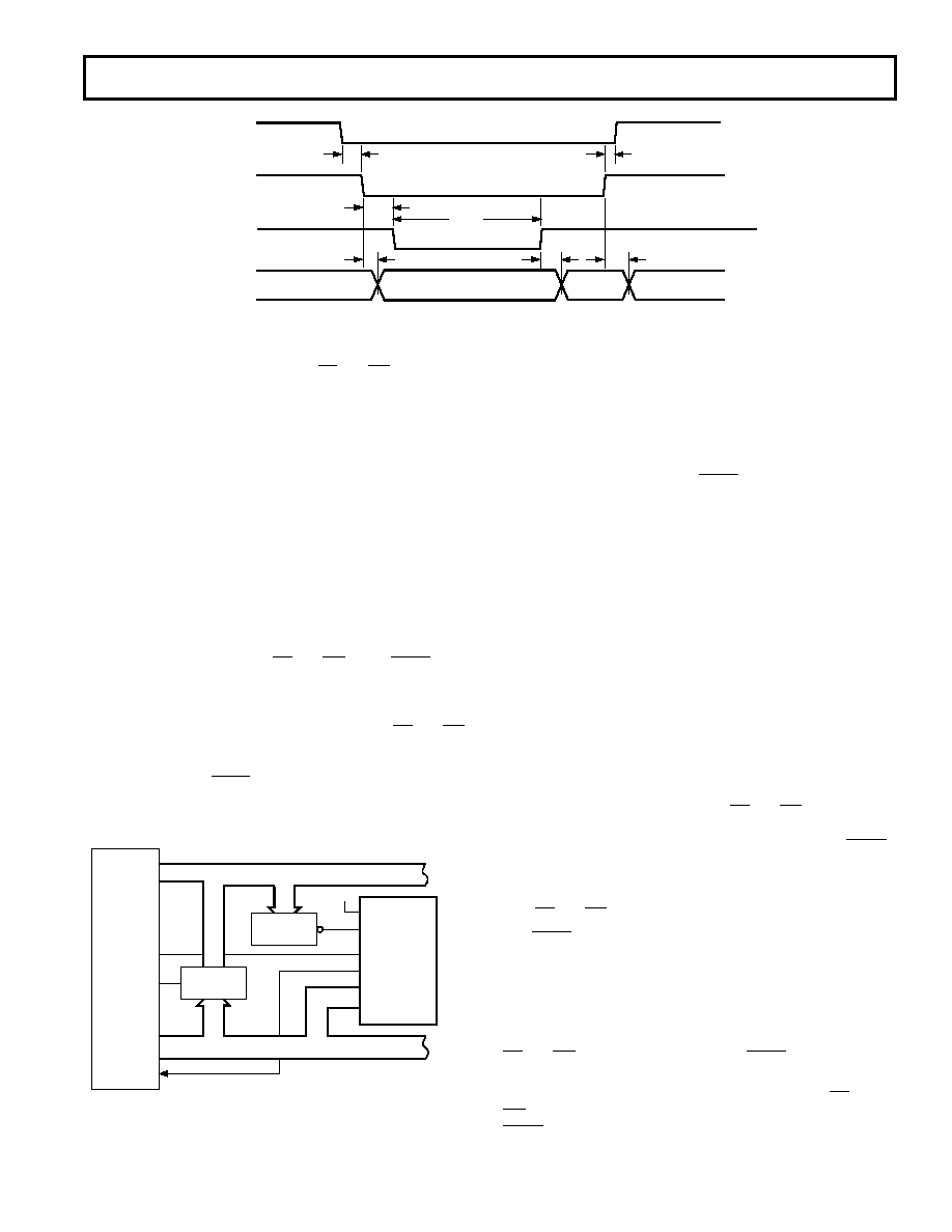
t5
t1
t2
t6
t7
tCONV
HIGH IMPEDANCE
BUS
NEW
DATA
OLD DATA
HIGH IMPEDANCE
BUS
CS
RD
BUSY
DATA
t3
Figure 3. Slow Memory Interface Timing Diagram
相关PDF资料 |
PDF描述 |
|---|---|
| MS27467E13A35SB | CONN PLUG 22POS STRAIGHT W/SCKT |
| VE-JW2-MX-S | CONVERTER MOD DC/DC 15V 75W |
| MS3106R28-21PW | CONN PLUG 37POS STRAIGHT W/PINS |
| SF7281-8PG-3ES | CONN RCPT 8POS PNL MNT PIN |
| VE-2NB-CU-F1 | CONVERTER MOD DC/DC 95V 200W |
相关代理商/技术参数 |
参数描述 |
|---|---|
| AD7575KPZ-REEL | 功能描述:IC ADC 8BIT LC2MOS W/HOLD 20PLCC RoHS:是 类别:集成电路 (IC) >> 数据采集 - 模数转换器 系列:- 产品培训模块:Lead (SnPb) Finish for COTS Obsolescence Mitigation Program 标准包装:2,500 系列:- 位数:12 采样率(每秒):3M 数据接口:- 转换器数目:- 功率耗散(最大):- 电压电源:- 工作温度:- 安装类型:表面贴装 封装/外壳:SOT-23-6 供应商设备封装:SOT-23-6 包装:带卷 (TR) 输入数目和类型:- |
| AD7575TCHIPS | 功能描述:8 Bit Analog to Digital Converter 1 Input 1 SAR Die 制造商:analog devices inc. 系列:- 包装:托盘 - 晶粒 零件状态:上次购买时间 位数:8 采样率(每秒):- 输入数:1 输入类型:单端 数据接口:并联 配置:S/H-ADC 无线电 - S/H:ADC:1:1 A/D 转换器数:1 架构:SAR 参考类型:外部 电压 - 电源,模拟:5V 电压 - 电源,数字:5V 特性:- 工作温度:-55°C ~ 125°C 封装/外壳:模具 供应商器件封装:模具 标准包装:1 |
| AD7576AQ | 制造商:Rochester Electronics LLC 功能描述:- Bulk 制造商:Analog Devices 功能描述: |
| AD7576BQ | 制造商:Rochester Electronics LLC 功能描述:- Bulk |
| AD7576JN | 制造商:Rochester Electronics LLC 功能描述:- Bulk 制造商:Analog Devices 功能描述:IC 8BIT ADC 7576 DIP18 |
发布紧急采购,3分钟左右您将得到回复。