参数资料
| 型号: | AD7606BSTZ-6 |
| 厂商: | Analog Devices Inc |
| 文件页数: | 7/36页 |
| 文件大小: | 0K |
| 描述: | IC DAS W/ADC 16BIT 6CH 64LQFP |
| 设计资源: | Layout Considerations for an Expandable Multichannel Simultaneous Sampling Data Acquisition System Based on AD7606 (CN0148) |
| 标准包装: | 1 |
| 类型: | 数据采集系统(DAS),ADC |
| 分辨率(位): | 16 b |
| 采样率(每秒): | 200k |
| 数据接口: | DSP,MICROWIRE?,并联,QSPI?,串行,SPI? |
| 电压电源: | 模拟和数字 |
| 电源电压: | 2.3 V ~ 5.25 V,4.75 V ~ 5.25 V |
| 工作温度: | -40°C ~ 85°C |
| 安装类型: | 表面贴装 |
| 封装/外壳: | 64-LQFP |
| 供应商设备封装: | 64-LQFP(10x10) |
| 包装: | 托盘 |
第1页第2页第3页第4页第5页第6页当前第7页第8页第9页第10页第11页第12页第13页第14页第15页第16页第17页第18页第19页第20页第21页第22页第23页第24页第25页第26页第27页第28页第29页第30页第31页第32页第33页第34页第35页第36页
Data Sheet
AD7606/AD7606-6/AD7606-4
Rev. C | Page 15 of 36
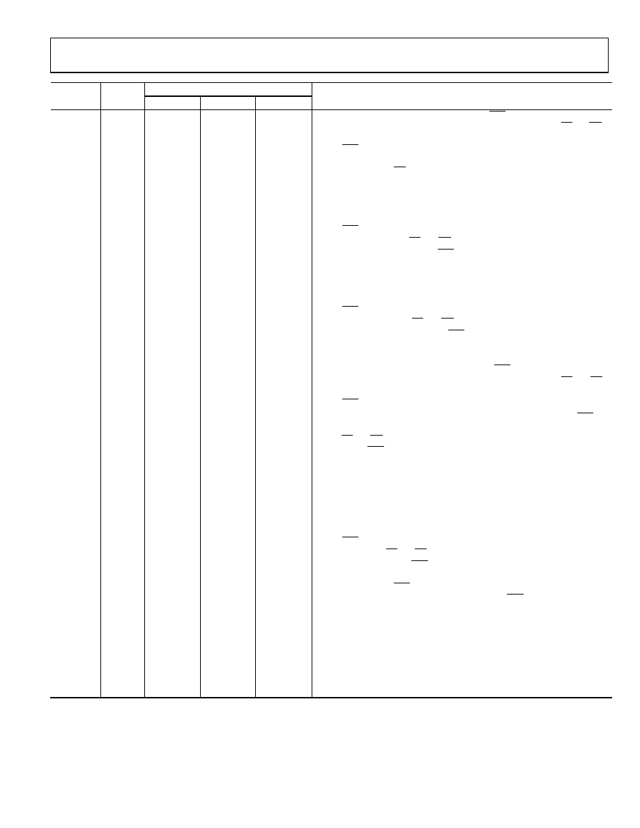
Pin No.
Type1
Mnemonic
Description
AD7606
AD7606-6
AD7606-4
22 to 16
DO
DB[6:0]
Parallel Output Data Bits, DB6 to DB0. When PAR/SER/BYTE SEL = 0, these
pins act as three-state parallel digital input/output pins. When CS and RD
are low, these pins are used to output DB6 to DB0 of the conversion result.
When PAR/SER/BYTE SEL = 1, these pins should be tied to AGND. When
operating in parallel byte interface mode, DB[7:0] outputs the 16-bit con-
version result in two RD operations. DB7 (Pin 24) is the MSB; DB0 is the LSB.
23
P
VDRIVE
Logic Power Supply Input. The voltage (2.3 V to 5.25 V) supplied at this pin
determines the operating voltage of the interface. This pin is nominally at the
same supply as the supply of the host interface (that is, DSP and FPGA).
24
DO
DB7/DOUTA
Parallel Output Data Bit 7 (DB7)/Serial Interface Data Output Pin (DOUTA).
When PAR/SER/BYTE SEL = 0, this pins acts as a three-state parallel digital
input/output pin. When CS and RD are low, this pin is used to output DB7
of the conversion result. When PAR/SER/BYTE SEL = 1, this pin functions
section for more details). When operating in parallel byte mode, DB7 is
the MSB of the byte.
25
DO
DB8/DOUTB
Parallel Output Data Bit 8 (DB8)/Serial Interface Data Output Pin (DOUTB).
When PAR/SER/BYTE SEL = 0, this pin acts as a three-state parallel digital
input/output pin. When CS and RD are low, this pin is used to output
DB8 of the conversion result. When PAR/SER/BYTE SEL = 1, this pin functions
section for more details).
31 to 27
DO
DB[13:9]
Parallel Output Data Bits, DB13 to DB9. When PAR/SER/BYTE SEL = 0, these
pins act as three-state parallel digital input/output pins. When CS and RD
are low, these pins are used to output DB13 to DB9 of the conversion result.
When PAR/SER/BYTE SEL = 1, these pins should be tied to AGND.
32
DO/DI
DB14/
HBEN
DB14/
HBEN
DB14/
HBEN
Parallel Output Data Bit 14 (DB14)/High Byte Enable (HBEN). When PAR/
SER/BYTE SEL = 0, this pin acts as a three-state parallel digital output pin.
When CS and RD are low, this pin is used to output DB14 of the conversion
result. When PAR/SER/BYTE SEL = 1 and DB15/BYTE SEL = 1, the AD7606/
AD7606-6/AD7606-4 operate in parallel byte interface mode. In parallel
byte mode, the HBEN pin is used to select whether the most significant byte
(MSB) or the least significant byte (LSB) of the conversion result is output first.
When HBEN = 1, the MSB is output first, followed by the LSB.
When HBEN = 0, the LSB is output first, followed by the MSB.
In serial mode, this pin should be tied to GND.
33
DO/DI
DB15/
BYTE SEL
DB15/
BYTE SEL
DB15/
BYTE SEL
Parallel Output Data Bit 15 (DB15)/Parallel Byte Mode Select (BYTE SEL).
When PAR/SER/BYTE SEL = 0, this pin acts as a three-state parallel digital
output pin. When CS and RD are low, this pin is used to output DB15 of the
conversion result. When PAR/SER/BYTE SEL = 1, the BYTE SEL pin is used to
select between serial interface mode and parallel byte interface mode
(see Table 8). When PAR/SER/BYTE SEL = 1 and DB15/BYTE SEL = 0, the
AD7606 operates in serial interface mode. When PAR/SER/BYTE SEL = 1
and DB15/BYTE SEL = 1, the AD7606 operates in parallel byte interface mode.
34
DI
REF SELECT
Internal/External Reference Selection Input. Logic input. If this pin is set to
logic high, the internal reference is selected and enabled. If this pin is set to
logic low, the internal reference is disabled and an external reference
voltage must be applied to the REFIN/REFOUT pin.
36, 39
P
REGCAP
Decoupling Capacitor Pin for Voltage Output from Internal Regulator.
These output pins should be decoupled separately to AGND using a 1 μF
capacitor. The voltage on these pins is in the range of 2.5 V to 2.7 V.
相关PDF资料 |
PDF描述 |
|---|---|
| AD2S1210CSTZ | IC CONV R/D VAR RES OSC 48-LQFP |
| VI-24P-MY-S | CONVERTER MOD DC/DC 13.8V 50W |
| AD7607BSTZ | IC DAS W/ADC 14BIT 8CH 64LQFP |
| V110A5M200BG3 | CONVERTER MOD DC/DC 5V 200W |
| VI-24N-MY-S | CONVERTER MOD DC/DC 18.5V 50W |
相关代理商/技术参数 |
参数描述 |
|---|---|
| AD7606BSTZ-6RL | 功能描述:IC DAS W/ADC 16BIT 64LQFP RoHS:是 类别:集成电路 (IC) >> 数据采集 - ADCs/DAC - 专用型 系列:- 产品培训模块:Lead (SnPb) Finish for COTS Obsolescence Mitigation Program 标准包装:50 系列:- 类型:数据采集系统(DAS) 分辨率(位):16 b 采样率(每秒):21.94k 数据接口:MICROWIRE?,QSPI?,串行,SPI? 电压电源:模拟和数字 电源电压:1.8 V ~ 3.6 V 工作温度:-40°C ~ 85°C 安装类型:表面贴装 封装/外壳:40-WFQFN 裸露焊盘 供应商设备封装:40-TQFN-EP(6x6) 包装:托盘 |
| AD7606BSTZ-RL | 功能描述:IC DAS W/ADC 16BIT 64LQFP RoHS:是 类别:集成电路 (IC) >> 数据采集 - ADCs/DAC - 专用型 系列:- 产品培训模块:Lead (SnPb) Finish for COTS Obsolescence Mitigation Program 标准包装:50 系列:- 类型:数据采集系统(DAS) 分辨率(位):16 b 采样率(每秒):21.94k 数据接口:MICROWIRE?,QSPI?,串行,SPI? 电压电源:模拟和数字 电源电压:1.8 V ~ 3.6 V 工作温度:-40°C ~ 85°C 安装类型:表面贴装 封装/外壳:40-WFQFN 裸露焊盘 供应商设备封装:40-TQFN-EP(6x6) 包装:托盘 |
| AD7607 | 制造商:AD 制造商全称:Analog Devices 功能描述:8-Channel Differential DAS with 18-Bit, Bipolar, Simultaneous Sampling ADC |
| AD7607BSTZ | 功能描述:IC DAS W/ADC 14BIT 8CH 64LQFP RoHS:是 类别:集成电路 (IC) >> 数据采集 - ADCs/DAC - 专用型 系列:- 产品培训模块:Lead (SnPb) Finish for COTS Obsolescence Mitigation Program 标准包装:50 系列:- 类型:数据采集系统(DAS) 分辨率(位):16 b 采样率(每秒):21.94k 数据接口:MICROWIRE?,QSPI?,串行,SPI? 电压电源:模拟和数字 电源电压:1.8 V ~ 3.6 V 工作温度:-40°C ~ 85°C 安装类型:表面贴装 封装/外壳:40-WFQFN 裸露焊盘 供应商设备封装:40-TQFN-EP(6x6) 包装:托盘 |
| AD7607BSTZ-RL | 功能描述:IC DAS W/ADC 14BIT 8CH 64LQFP RoHS:是 类别:集成电路 (IC) >> 数据采集 - ADCs/DAC - 专用型 系列:- 产品培训模块:Lead (SnPb) Finish for COTS Obsolescence Mitigation Program 标准包装:50 系列:- 类型:数据采集系统(DAS) 分辨率(位):16 b 采样率(每秒):21.94k 数据接口:MICROWIRE?,QSPI?,串行,SPI? 电压电源:模拟和数字 电源电压:1.8 V ~ 3.6 V 工作温度:-40°C ~ 85°C 安装类型:表面贴装 封装/外壳:40-WFQFN 裸露焊盘 供应商设备封装:40-TQFN-EP(6x6) 包装:托盘 |
发布紧急采购,3分钟左右您将得到回复。