- 您现在的位置:买卖IC网 > PDF目录165343 > AD7609BSTZ-RL (ANALOG DEVICES INC) 8-CH 18-BIT SUCCESSIVE APPROXIMATION ADC, SERIAL/PARALLEL ACCESS, PQFP64 PDF资料下载
参数资料
| 型号: | AD7609BSTZ-RL |
| 厂商: | ANALOG DEVICES INC |
| 元件分类: | ADC |
| 英文描述: | 8-CH 18-BIT SUCCESSIVE APPROXIMATION ADC, SERIAL/PARALLEL ACCESS, PQFP64 |
| 封装: | ROHS COMPLIANT, MS-026BCD, LQFP-64 |
| 文件页数: | 18/35页 |
| 文件大小: | 1737K |
| 代理商: | AD7609BSTZ-RL |
第1页第2页第3页第4页第5页第6页第7页第8页第9页第10页第11页第12页第13页第14页第15页第16页第17页当前第18页第19页第20页第21页第22页第23页第24页第25页第26页第27页第28页第29页第30页第31页第32页第33页第34页第35页
Preliminary Technical Data
AD7609
Rev. PrD | Page 25 of 35
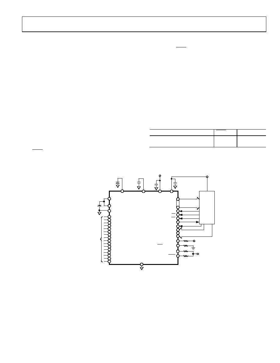
TYPICAL CONNECTION DIAGRAM
Figure 42 shows the typical connection diagram for the
AD7609. There are four AVCC supply pins on the part which
can be tied together and decoupled using a 100 nF capacitor at
each supply pin and a 10 μF capacitor at the supply source. The
AD7609 can operate with the internal reference or an externally
applied reference. In this configuration, the AD7609 is config-
ured to operate with the internal reference. When using a single
AD7609 device on the board, the REFIN/REFOUT pin should
be decoupled with a 10 μF capacitor, in an application with
multiple AD7609 devices see the Internal/External Reference
section. The REFCAPA and REFCAPB pins are shorted together
and decoupled with a 10 μF ceramic capacitor.
The VDRIVE supply is connected to the same supply as the pro-
cessor. The voltage on VDRIVE controls the voltage value of the
output logic signals. For layout, decoupling, and grounding
hints, see the Layout Guidelines section.
POWER-DOWN MODES
There are two power-down modes available on the AD7609.
The STBY pin controls whether the AD7609 is in normal mode
or one of the two power-down modes. The two power-down
modes available are standby mode and shutdown mode. The
power-down mode is selected through the state of the RANGE
pin when the STBY pin is low.
shows the configurations
required to choose the desired power-down mode. When the
AD7609 is placed in standby mode the current consumption is
2 mA maximum and power up time is approximately 100 μs as
the capacitor on the REFCAPA/REFCAPB pins must charge up.
In standby mode, the on-chip reference and regulators remain
powered up and the amplifiers and ADC core are powered
down. When the AD7609 is placed in shutdown mode, the
current consumption is 1 μA maximum and power up time
is also in the order of 11 ms. In shutdown mode, all circuitry
is powered down. When the AD7609 is powered up from
shutdown mode, a reset signal must be applied to the AD7609
after the required power up time has elapsed.
Table 8 Power-Down Mode Selection
Power-Down Mode
STBY
RANGE
Standby
0
1
Shutdown
0
AVCC
AGND
VDRIVE
+
REFIN/REFOUT
DB0 TO DB15
CONVST A, B
CS
RD
BUSY
RESET
AD7609
1F
10F
100nF
DIGITAL SUPPLY
VOLTAGE +2.3V TO +5V
ANALOG SUPPLY
VOLTAGE 5V1
EIGHT DIFFERENTIAL
ANALOG INPUT PAIRS
PARALLEL
INTERFACE
1DECOUPLING SHOWN ON THE AVCC PIN APPLIES TO EACH AVCC PIN (PIN 1, PIN 37, PIN 38, PIN 48).
DECOUPLING CAPACITOR CAN BE SHARED BETWEEN AVCC PIN 37 AND PIN 38.
2DECOUPLING SHOWN ON THE REGCAP PIN APPLIES TO EACH REGCAP PIN (PIN 36, PIN 39).
REGCAP2
+
10F
REFCAPA
REFCAPB
OS 2
OS 1
OS 0
OVERSAMPLING
100nF
V1+
PAR/SER SEL
STBY
REF SELECT
RANGE
V2+
V3+
V4+
V5+
V6+
V7+
V8+
REFGND
V1–
V2–
V3–
V4–
V5–
V6–
V7–
V8–
VDRIVE
M
IC
R
O
PR
O
C
E
SSO
R
/
M
ICRO
CO
NV
E
RT
E
R/
DS
P
09
76
0-
0
38
Figure 42. AD7609 Typical Connection Diagram
相关PDF资料 |
PDF描述 |
|---|---|
| AD7609BSTZ | 8-CH 18-BIT SUCCESSIVE APPROXIMATION ADC, SERIAL/PARALLEL ACCESS, PQFP64 |
| AD7746 | DIGITAL TEMP SENSOR-SERIAL, 24BIT(s), 2Cel, RECTANGULAR, SURFACE MOUNT |
| AD7811YRUZ | 4-CH 10-BIT SUCCESSIVE APPROXIMATION ADC, SERIAL ACCESS, PDSO16 |
| AD7845KRZ | PARALLEL, WORD INPUT LOADING, 2.5 us SETTLING TIME, 12-BIT DAC, PDSO24 |
| AD7911ARMZ-REEL | 2-CH 10-BIT SUCCESSIVE APPROXIMATION ADC, SERIAL ACCESS, PDSO8 |
相关代理商/技术参数 |
参数描述 |
|---|---|
| AD760AN | 制造商:未知厂家 制造商全称:未知厂家 功能描述:16-Bit Digital-to-Analog Converter |
| AD760AP | 制造商:未知厂家 制造商全称:未知厂家 功能描述:16-Bit Digital-to-Analog Converter |
| AD760AQ | 功能描述:IC DAC 16BIT W/AMP SRL 28-CDIP RoHS:否 类别:集成电路 (IC) >> 数据采集 - 数模转换器 系列:DACPORT® 产品培训模块:Lead (SnPb) Finish for COTS Obsolescence Mitigation Program 标准包装:50 系列:- 设置时间:4µs 位数:12 数据接口:串行 转换器数目:2 电压电源:单电源 功率耗散(最大):- 工作温度:-40°C ~ 85°C 安装类型:表面贴装 封装/外壳:8-TSSOP,8-MSOP(0.118",3.00mm 宽) 供应商设备封装:8-uMAX 包装:管件 输出数目和类型:2 电压,单极 采样率(每秒):* 产品目录页面:1398 (CN2011-ZH PDF) |
| AD760SQ | 制造商:未知厂家 制造商全称:未知厂家 功能描述:16-Bit Digital-to-Analog Converter |
| AD7610 | 制造商:AD 制造商全称:Analog Devices 功能描述:14-Bit, 1 MSPS, Differential, Programmable Input PulSAR ADC |
发布紧急采购,3分钟左右您将得到回复。