- 您现在的位置:买卖IC网 > PDF目录10526 > AD7623ASTZ (Analog Devices Inc)IC ADC 16BIT 1.33MSPS DFF 48LQFP PDF资料下载
参数资料
| 型号: | AD7623ASTZ |
| 厂商: | Analog Devices Inc |
| 文件页数: | 9/28页 |
| 文件大小: | 0K |
| 描述: | IC ADC 16BIT 1.33MSPS DFF 48LQFP |
| 标准包装: | 1 |
| 系列: | PulSAR® |
| 位数: | 16 |
| 采样率(每秒): | 1.33M |
| 数据接口: | 串行,并联 |
| 转换器数目: | 1 |
| 功率耗散(最大): | 55mW |
| 电压电源: | 模拟和数字 |
| 工作温度: | -40°C ~ 85°C |
| 安装类型: | 表面贴装 |
| 封装/外壳: | 48-LQFP |
| 供应商设备封装: | 48-LQFP(7x7) |
| 包装: | 托盘 |
| 输入数目和类型: | 1 个差分,双极 |
| 配用: | EVAL-AD7623CBZ-ND - BOARD EVALUATION FOR AD7623 |
第1页第2页第3页第4页第5页第6页第7页第8页当前第9页第10页第11页第12页第13页第14页第15页第16页第17页第18页第19页第20页第21页第22页第23页第24页第25页第26页第27页第28页
AD7623
Rev. 0 | Page 17 of 28
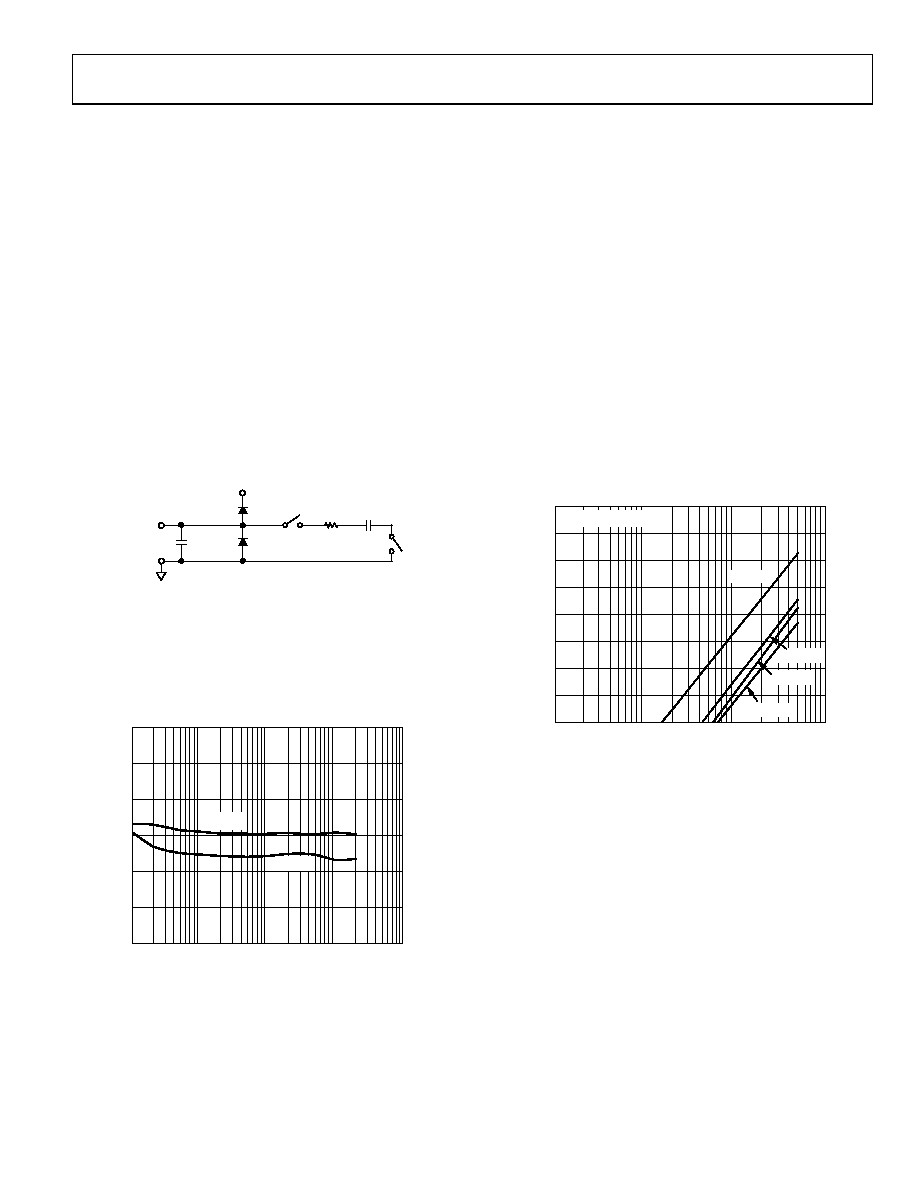
TYPICAL CONNECTION DIAGRAM
Figure 23 shows a typical connection diagram for the AD7623.
Different circuitry from that shown in this diagram are optional
and are discussed in the Analog Inputs section.
ANALOG INPUTS
Figure 24 shows an equivalent circuit of the input structure of
the AD7623.
The two diodes, D1 and D2, provide ESD protection for the
analog inputs, IN+ and IN. Care must be taken to ensure that
the analog input signal never exceeds the supply rails by more
than 0.3 V, because this causes the diodes to become forward-
biased and to start conducting current. These diodes can handle
a forward-biased current of 100 mA maximum. For instance,
these conditions could eventually occur when the input buffer’s
U1 or U2 supplies are different from AVDD. In such a case, an
input buffer with a short-circuit current limitation can be used
to protect the part.
05574-024
D1
RIN
CIN
D2
IN+ OR IN–
AGND
AVDD
CPIN
Figure 24. AD7623 Simplified Analog Input
The analog inputs of the AD7623 are a true differential
structure. By using this differential input, small signals common
to both inputs are rejected, as shown in Figure 25, representing
the typical CMRR over frequency with internal and external
references.
05574-025
FREQUENCY (kHz)
CMRR
(dB)
45
75
70
65
60
55
50
1
10
100
1000
10000
EXT REF
INT REF
Figure 25. Analog Input CMRR vs. Frequency
During the acquisition phase for ac signals, the impedance of
the analog inputs, IN+ and IN, can be modeled as a parallel
combination of Capacitor CPIN and the network formed by the
series connection of RIN and CIN. CPIN is primarily the pin
capacitance. RIN is typically 350 Ω and is a lumped component
comprised of some serial resistors and the on resistance of the
switches. CIN is typically 12 pF and is primarily the ADC
sampling capacitor. During the conversion phase, when the
switches are opened, the input impedance is limited to CPIN. RIN
and CIN make a one-pole, low-pass filter that has a typical 3 dB
cutoff frequency of 50 MHz, thereby reducing an undesirable
aliasing effect while limiting noise from the inputs.
Since the input impedance of the AD7623 is very high, the
AD7623 can be directly driven by a low impedance source
without gain error. To further improve the noise filtering
achieved by the AD7623 analog input circuit, an external,
one-pole RC filter between the amplifier’s outputs and the ADC
analog inputs can be used, as shown in Figure 23. However,
large source impedances significantly affect the ac performance,
especially total harmonic distortion (THD). The maximum
source impedance depends on the amount of THD that can be
tolerated. The THD degrades as a function of the source
impedance and the maximum input frequency, as shown in
05574-026
INPUT FREQUENCY (kHz)
THD
(dB)
–100
–60
–65
–70
–75
–80
–85
–90
–95
1
10
100
1k
RS = 500Ω
RS = 50Ω
RS = 100Ω
RS = 10Ω
PDBUF = PDREF = LOW
Figure 26. THD vs. Analog Input Frequency and Source Resistance
DRIVER AMPLIFIER CHOICE
Although the AD7623 is easy to drive, the driver amplifier must
meet the following requirements:
Together, the driver amplifier and the AD7623 analog
input circuit must be able to settle for a full-scale step of
the capacitor array at a 16-bit level (0.0015%). In the
amplifier data sheet, settling at 0.1% to 0.01% is more
commonly specified. This could differ significantly from
the settling time at a 16-bit level and should be verified
prior to driver selection. The AD8021 op amp, which
combines ultralow noise and high gain bandwidth, meets
this settling time requirement even when used with gains
up to 13.
The noise generated by the driver amplifier needs to be
kept as low as possible to preserve the SNR and transition
noise performance of the AD7623. The noise coming from
the driver is filtered by the AD7623 analog input circuit
相关PDF资料 |
PDF描述 |
|---|---|
| MS3102A22-23SY | CONN RCPT 8POS BOX MNT W/SCKT |
| AD976ARSZ | IC ADC 16BIT 100KSPS 28-SSOP |
| MS3102A22-23S | CONN RCPT 8POS BOX MNT W/SCKT |
| AD976ARZ | IC ADC 16BIT 100KSPS 28-SOIC |
| MS3102A22-17S | CONN RCPT 9POS BOX MNT W/SCKT |
相关代理商/技术参数 |
参数描述 |
|---|---|
| AD7623ASTZRL | 功能描述:IC ADC 16BIT 1.33MSPS DFF 48LQFP RoHS:是 类别:集成电路 (IC) >> 数据采集 - 模数转换器 系列:PulSAR® 标准包装:1 系列:- 位数:14 采样率(每秒):83k 数据接口:串行,并联 转换器数目:1 功率耗散(最大):95mW 电压电源:双 ± 工作温度:0°C ~ 70°C 安装类型:通孔 封装/外壳:28-DIP(0.600",15.24mm) 供应商设备封装:28-PDIP 包装:管件 输入数目和类型:1 个单端,双极 |
| AD7623BD | 制造商:INTERSIL 制造商全称:Intersil Corporation 功能描述:Data Acquisition |
| AD7625 | 制造商:AD 制造商全称:Analog Devices 功能描述:16-Bit, 6MSPS PulSAR Differential ADC |
| AD7625BCPZ | 功能描述:IC ADC 16BIT 6MSPS SAR 32LFCSP RoHS:是 类别:集成电路 (IC) >> 数据采集 - 模数转换器 系列:PulSAR® 其它有关文件:TSA1204 View All Specifications 标准包装:1 系列:- 位数:12 采样率(每秒):20M 数据接口:并联 转换器数目:2 功率耗散(最大):155mW 电压电源:模拟和数字 工作温度:-40°C ~ 85°C 安装类型:表面贴装 封装/外壳:48-TQFP 供应商设备封装:48-TQFP(7x7) 包装:Digi-Reel® 输入数目和类型:4 个单端,单极;2 个差分,单极 产品目录页面:1156 (CN2011-ZH PDF) 其它名称:497-5435-6 |
| AD7625BCPZRL7 | 功能描述:IC ADC 16BIT 6MSPS SAR 32LFCSP RoHS:是 类别:集成电路 (IC) >> 数据采集 - 模数转换器 系列:PulSAR® 标准包装:1 系列:- 位数:14 采样率(每秒):83k 数据接口:串行,并联 转换器数目:1 功率耗散(最大):95mW 电压电源:双 ± 工作温度:0°C ~ 70°C 安装类型:通孔 封装/外壳:28-DIP(0.600",15.24mm) 供应商设备封装:28-PDIP 包装:管件 输入数目和类型:1 个单端,双极 |
发布紧急采购,3分钟左右您将得到回复。