参数资料
| 型号: | AD7628KPZ |
| 厂商: | Analog Devices Inc |
| 文件页数: | 6/8页 |
| 文件大小: | 0K |
| 描述: | IC DAC 8BIT DUAL MULTIPLY 20PLCC |
| 标准包装: | 49 |
| 设置时间: | 400ns |
| 位数: | 8 |
| 转换器数目: | 2 |
| 电压电源: | 单电源 |
| 功率耗散(最大): | 450mW |
| 工作温度: | -40°C ~ 85°C |
| 安装类型: | 表面贴装 |
| 封装/外壳: | 20-LCC(J 形引线) |
| 供应商设备封装: | 20-PLCC(9x9) |
| 包装: | 管件 |
| 输出数目和类型: | 2 电流,单极;2 电流,双极 |
| 采样率(每秒): | 2.9M |
AD7628
–6–
REV. A
APPLICATIONS INFORMATION
Application Hints
To ensure system performance consistent with AD7628 specifi-
cations, careful attention must be given to the following points:
1. GENERAL GROUND MANAGEMENT: AC or transient
voltages between the AD7628 AGND and DGND can cause
noise injection into the analog output. The simplest method
of ensuring that voltages at AGND and DGND are equal is
to tie AGND and DGND together at the AD7628. In more
omplex systems where the AGND–DGND intertie is on the
backplane, it is recommended that diodes be connected in
inverse parallel between the AD7628 AGND and DGND
pins (1N914 or equivalent).
2. OUTPUT AMPLIFIER OFFSET: CMOS DACs exhibit a
code-dependent output resistance which, in turn, causes a
code-dependent amplifier noise gain. The effect is a code-
dependent differential nonlinearity term at the amplifier
output that depends on VOS (VOS is amplifier input offset
voltage). This differential nonlinearity term adds to the R/2R
differential nonlinearity. To maintain monotonic operation, it
is recommended that amplifier VOS be no greater than 10% of
1 LSB over the temperature range of interest.
3. HIGH FREQUENCY CONSIDERATIONS: The output
capacitance of a CMOS DAC works in conjunction with the
amplifier feedback resistance to add a pole to the open loop
response. This can cause ringing or oscillation. Stability can
be restored by adding a phase compensation capacitor in
parallel with the feedback resistor.
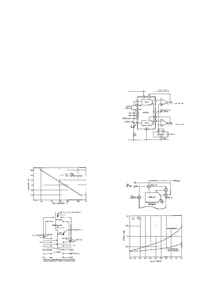
DYNAMIC PERFORMANCE
The dynamic performance of the two DACs in the AD7628 will
depend on the gain and phase characteristics of the output am-
plifiers, together with the optimum choice of the PC board lay-
out and decoupling components. Figure 6 shows the relationship
between input frequency and channel-to-channel isolation.
Figure 6. Channel-to-Channel Isolation
Figure 7. Suggested PC Board Layout for AD7628 with
AD644 Dual Op Amp
Figure 7 shows a printed circuit layout for the AD7628 and the
AD644 dual op amp, which minimizes feedthrough and crosstalk.
SINGLE SUPPLY APPLICATIONS
The AD7628 DAC R-2R ladder termination resistors are con-
nected to AGND within the device. This arrangement is par-
ticularly convenient for single supply operation because AGND
may be biased at any voltage between DGND and VDD. Figure
8 shows a circuit that provides two +5 V to +8 V analog outputs
by biasing AGND +5 V up from DGND. The two DAC refer-
ence inputs are tied together and a reference input voltage is ob-
tained without a buffer amplifier by making use of the constant
and matched impedances of the DAC A and DAC B reference
inputs. Current flows through the two DAC R-2R ladders into
R1, and R1 is adjusted until the VREF A and VREF B inputs are
at +2 V. The two analog output voltages range from +5 V to
+8 V for DAC codes 00000000 to l l l l l l l l .
Figure 8. AD7628 Single Supply Operation
Figure 9 shows DAC A of the AD7628 connected in a positive
reference, voltage switching mode. This configuration is useful
because VOUT is the same polarity as VIN, allowing single supply
operation. However, to retain specified linearity, VIN must be in
the range 0 V to +2.5 V and the output buffered or loaded with
a high impedance (see Figure 10). Note that the input voltage is
connected to the DAC OUT A, and the output voltage is taken
from the DAC VREF A pin.
Figure 9. AD7628 Single Supply, Voltage Switching Mode
Figure 10. Typical AD7628 Performance in Single Supply
Voltage Switching Mode
相关PDF资料 |
PDF描述 |
|---|---|
| AD7303BNZ | IC DAC 8BIT DUAL R-R 8-DIP |
| VI-2NK-MW-F2 | CONVERTER MOD DC/DC 40V 100W |
| VI-JTL-MZ-F2 | CONVERTER MOD DC/DC 28V 25W |
| VI-20V-MY-F1 | CONVERTER MOD DC/DC 5.8V 50W |
| VI-2NK-MW-F1 | CONVERTER MOD DC/DC 40V 100W |
相关代理商/技术参数 |
参数描述 |
|---|---|
| AD7628KPZ-REEL | 功能描述:IC DAC 8BIT DUAL MULTIPLY 20PLCC RoHS:是 类别:集成电路 (IC) >> 数据采集 - 数模转换器 系列:- 产品培训模块:LTC263x 12-, 10-, and 8-Bit VOUT DAC Family 特色产品:LTC2636 - Octal 12-/10-/8-Bit SPI VOUT DACs with 10ppm/°C Reference 标准包装:91 系列:- 设置时间:4µs 位数:10 数据接口:MICROWIRE?,串行,SPI? 转换器数目:8 电压电源:单电源 功率耗散(最大):2.7mW 工作温度:-40°C ~ 85°C 安装类型:表面贴装 封装/外壳:14-WFDFN 裸露焊盘 供应商设备封装:14-DFN-EP(4x3) 包装:管件 输出数目和类型:8 电压,单极 采样率(每秒):* |
| AD7628KR | 功能描述:IC DAC 8BIT DUAL MULTIPLY 20SOIC RoHS:否 类别:集成电路 (IC) >> 数据采集 - 数模转换器 系列:- 标准包装:2,400 系列:- 设置时间:- 位数:18 数据接口:串行 转换器数目:3 电压电源:模拟和数字 功率耗散(最大):- 工作温度:-40°C ~ 85°C 安装类型:表面贴装 封装/外壳:36-TFBGA 供应商设备封装:36-TFBGA 包装:带卷 (TR) 输出数目和类型:* 采样率(每秒):* |
| AD7628KR-REEL | 制造商:Analog Devices 功能描述: |
| AD7628KRZ | 功能描述:IC DAC 8BIT DUAL W/BUFF 20-SOIC RoHS:是 类别:集成电路 (IC) >> 数据采集 - 数模转换器 系列:- 产品培训模块:LTC263x 12-, 10-, and 8-Bit VOUT DAC Family 特色产品:LTC2636 - Octal 12-/10-/8-Bit SPI VOUT DACs with 10ppm/°C Reference 标准包装:91 系列:- 设置时间:4µs 位数:10 数据接口:MICROWIRE?,串行,SPI? 转换器数目:8 电压电源:单电源 功率耗散(最大):2.7mW 工作温度:-40°C ~ 85°C 安装类型:表面贴装 封装/外壳:14-WFDFN 裸露焊盘 供应商设备封装:14-DFN-EP(4x3) 包装:管件 输出数目和类型:8 电压,单极 采样率(每秒):* |
| AD7628KRZ | 制造商:Analog Devices 功能描述:IC 8-BIT DAC |
发布紧急采购,3分钟左右您将得到回复。