参数资料
| 型号: | AD7651ACPZ |
| 厂商: | Analog Devices Inc |
| 文件页数: | 11/28页 |
| 文件大小: | 0K |
| 描述: | IC ADC 16BIT UNIPOLAR 48LFCSP |
| 标准包装: | 1 |
| 系列: | PulSAR® |
| 位数: | 16 |
| 采样率(每秒): | 100k |
| 数据接口: | 串行,并联 |
| 转换器数目: | 1 |
| 功率耗散(最大): | 45mW |
| 电压电源: | 模拟和数字 |
| 工作温度: | -40°C ~ 85°C |
| 安装类型: | 表面贴装 |
| 封装/外壳: | 48-VFQFN 裸露焊盘,CSP |
| 供应商设备封装: | 48-LFCSP-VQ(7x7) |
| 包装: | 托盘 |
| 输入数目和类型: | 2 个伪差分,单极 |
| 配用: | EVAL-AD7651CBZ-ND - BOARD EVALUATION FOR AD7651 |
第1页第2页第3页第4页第5页第6页第7页第8页第9页第10页当前第11页第12页第13页第14页第15页第16页第17页第18页第19页第20页第21页第22页第23页第24页第25页第26页第27页第28页
AD7651
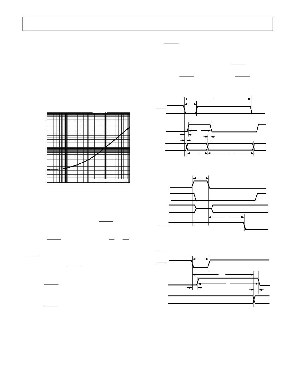
POWER DISSIPATION VERSUS THROUGHPUT
The CNVST trace should be shielded with ground and a low
value serial resistor (i.e., 50 ) termination should be added
close to the output of the component that drives this line.
Operating currents are very low during the acquisition phase,
allowing significant power savings when the conversion rate is
reduced (see
). The AD7651 automatically reduces its
power consumption at the end of each conversion phase. This
makes the part ideal for very low power battery applications.
The digital interface and the reference remain active even
during the acquisition phase. To reduce operating digital supply
currents even further, digital inputs need to be driven close to
the power supply rails (i.e., DVDD or DGND), and OVDD
should not exceed DVDD by more than 0.3 V.
Figure 25. Power Dissipation vs. Sampling Rate
For applications where SNR is critical, the CNVST signal should
have very low jitter. This may be achieved by using a dedicated
oscillator for CNVST generation, or to clock CNVST with a
high frequency, low jitter clock, as shown in
BUSY
MODE
t2
t1
t3
t4
t5
t6
t7
t8
ACQUIRE
CONVERT
ACQUIRE
CONVERT
02964-0-011
CNVST
100000
POW
E
R
D
ISSIPA
TION
(
W)
SAMPLING RATE (SPS)
100k
1k
10
100
10k
10000
1000
100
10
02964-0-038
PDREF = PDBUF = PDHIGH
CONVERSION CONTROL
Figure 26. Basic Conversion Timing
t9
t8
RESET
DATA
BUSY
02964-0-011
CNVST
shows the detailed timing diagrams of the conversion
process. The AD7651 is controlled by the CNVST signal, which
initiates conversion. Once initiated, it cannot be restarted or
aborted, even by the power-down input PD, until the conversion
is complete. CNVST operates independently of CS and RD.
Figure 27. RESET Timing
Conversions can be automatically initiated with the AD7651. If
CNVST is held LOW when BUSY is LOW, the AD7651 controls
the acquisition phase and automatically initiates a new
conversion. By keeping CNVST LOW, the AD7651 keeps the
conversion process running by itself. It should be noted that the
analog input must be settled when BUSY goes LOW. Also, at
power-up, CNVST should be brought LOW once to initiate the
conversion process. In this mode, the AD7651 can run slightly
faster than the guaranteed 100 kSPS.
t1
t3
t4
t11
BUSY
DATA
BUS
CS = RD = 0
t10
PREVIOUS CONVERSION DATA
NEW DATA
02964-0-012
CNVST
Although CNVST is a digital signal, it should be designed with
special care with fast, clean edges, and levels with minimum
overshoot and undershoot or ringing.
Figure 28. Master Parallel Data Timing for Reading (Continuous Read)
Rev. 0 | Page 19 of 28
相关PDF资料 |
PDF描述 |
|---|---|
| AD7652ASTZ | IC ADC 16BIT 500KSPS REF 48LQFP |
| AD7653ACPZRL | IC ADC 16BIT UNIPOLAR 48LFCSP |
| AD7654ACPZ | IC ADC 16BIT DUAL 2CH 48-LFCSP |
| AD7655ACPZRL | IC ADC 16BIT 4CHAN 48LFCSP |
| AD7656YSTZ-REEL | IC ADC 16BIT 6CH 250KSPS 64LQFP |
相关代理商/技术参数 |
参数描述 |
|---|---|
| AD7651ACPZRL | 功能描述:IC ADC 16BIT UNIPOLAR 48LQFP RoHS:是 类别:集成电路 (IC) >> 数据采集 - 模数转换器 系列:PulSAR® 标准包装:1,000 系列:- 位数:12 采样率(每秒):300k 数据接口:并联 转换器数目:1 功率耗散(最大):75mW 电压电源:单电源 工作温度:0°C ~ 70°C 安装类型:表面贴装 封装/外壳:24-SOIC(0.295",7.50mm 宽) 供应商设备封装:24-SOIC 包装:带卷 (TR) 输入数目和类型:1 个单端,单极;1 个单端,双极 |
| AD7651AST | 制造商:Rochester Electronics LLC 功能描述:16-BIT 100KSPS SAR UNIPOLAR ADC W/REEL - Tape and Reel 制造商:Analog Devices 功能描述: 制造商:Analog Devices 功能描述:16BIT SAR ADC REF 7651 LQFP48 |
| AD7651ASTRL | 制造商:Analog Devices 功能描述: |
| AD7651ASTZ | 功能描述:IC ADC 16BIT 100KSPS 48-LQFP RoHS:是 类别:集成电路 (IC) >> 数据采集 - 模数转换器 系列:PulSAR® 标准包装:1 系列:microPOWER™ 位数:8 采样率(每秒):1M 数据接口:串行,SPI? 转换器数目:1 功率耗散(最大):- 电压电源:模拟和数字 工作温度:-40°C ~ 125°C 安装类型:表面贴装 封装/外壳:24-VFQFN 裸露焊盘 供应商设备封装:24-VQFN 裸露焊盘(4x4) 包装:Digi-Reel® 输入数目和类型:8 个单端,单极 产品目录页面:892 (CN2011-ZH PDF) 其它名称:296-25851-6 |
| AD7651ASTZ | 制造商:Analog Devices 功能描述:16BIT SAR ADC REF 7651 LQFP48 |
发布紧急采购,3分钟左右您将得到回复。