- 您现在的位置:买卖IC网 > PDF目录10250 > AD7651ACPZRL (Analog Devices Inc)IC ADC 16BIT UNIPOLAR 48LQFP PDF资料下载
参数资料
| 型号: | AD7651ACPZRL |
| 厂商: | Analog Devices Inc |
| 文件页数: | 13/28页 |
| 文件大小: | 0K |
| 描述: | IC ADC 16BIT UNIPOLAR 48LQFP |
| 标准包装: | 2,500 |
| 系列: | PulSAR® |
| 位数: | 16 |
| 采样率(每秒): | 100k |
| 数据接口: | 串行,并联 |
| 转换器数目: | 1 |
| 功率耗散(最大): | 45mW |
| 电压电源: | 模拟和数字 |
| 工作温度: | -40°C ~ 85°C |
| 安装类型: | 表面贴装 |
| 封装/外壳: | 48-VFQFN 裸露焊盘,CSP |
| 供应商设备封装: | 48-LFCSP-VQ(7x7) |
| 包装: | 带卷 (TR) |
| 输入数目和类型: | 2 个伪差分,单极 |
| 配用: | EVAL-AD7651CBZ-ND - BOARD EVALUATION FOR AD7651 |
第1页第2页第3页第4页第5页第6页第7页第8页第9页第10页第11页第12页当前第13页第14页第15页第16页第17页第18页第19页第20页第21页第22页第23页第24页第25页第26页第27页第28页
AD7651
CURRENT
CONVERSION
BUSY
DATA
BUS
t12
t13
02964-0-013
RD
CS
DIGITAL INTERFACE
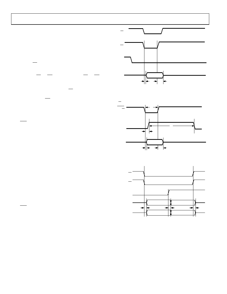
The AD7651 has a versatile digital interface; it can be interfaced
with the host system by using either a serial or a parallel
interface. The serial interface is multiplexed on the parallel data
bus. The AD7651 digital interface also accommodates both 3 V
and 5 V logic by simply connecting the OVDD supply pin of the
AD7651 to the host system interface digital supply. Finally, by
using the OB/2C input pin, both twos complement or straight
binary coding can be used.
The two signals, CS and RD, control the interface. CS and RD
have a similar effect because they are OR’d together internally.
When at least one of these signals is HIGH, the interface
outputs are in high impedance. Usually CS allows the selection
of each AD7651 in multicircuit applications and is held low in a
single AD7651 design. RD is generally used to enable the
conversion result on the data bus.
PARALLEL INTERFACE
The AD7651 is configured to use the parallel interface when
SER/PARis held LOW. The data can be read either after each
conversion, which is during the next acquisition phase, or
during the following conversion, as shown in F
, respectively. When the data is read during the
conversion, however, it is recommended that it is read only
during the first half of the conversion phase. This avoids any
potential feedthrough between voltage transients on the digital
interface and the most critical analog conversion circuitry.
Figure 29. Slave Parallel Data Timing for Reading (Read after Convert)
Figure 30. Slave Parallel Data Timing for Reading (Read during Convert)
PREVIOUS
CONVERSION
t1
t3
t12
t13
t4
BUSY
DATA
BUS
02964-0-014
CNVST,
RD
CS = 0
The BYTESWAP pin allows a glueless interface to an 8-bit bus.
As shown in
, the LSB byte is output on D[7:0] and the
MSB is output on D[15:8] when BYTESWAP is LOW. When
BYTESWAP is HIGH, the LSB and MSB bytes are swapped and
the LSB is output on D[15:8] and the MSB is output on D[7:0].
By connecting BYTESWAP to an address line, the 16-bit data
can be read in two bytes on either D[15:8] or D[7:0].
Figure 31. 8-Bit Parallel Interface
CS
RD
BYTESWAP
PINS D[15:8]
PINS D[7:0]
HI-Z
HIGH BYTE
LOW BYTE
HIGH BYTE
HI-Z
t12
t13
02964-0-025
SERIAL INTERFACE
The AD7651 is configured to use the serial interface when
SER/PAR is held HIGH. The AD7651 outputs 16 bits of data,
MSB first, on the SDOUT pin. This data is synchronized with
the 16 clock pulses provided on the SCLK pin. The output data
is valid on both the rising and falling edges of the data clock.
Rev. 0 | Page 20 of 28
相关PDF资料 |
PDF描述 |
|---|---|
| CS5532-BSZR | IC ADC 24BIT 2CH W/LNA 20-SSOP |
| LTC1851IFW#PBF | IC ADC 12BIT 1.25MSPS 48-TSSOP |
| LTC1851IFW | IC ADC 12BIT 1.25MSPS 48-TSSOP |
| MS27467T11A35PB | CONN PLUG 13POS STRAIGHT W/PINS |
| LTC1853IFW#PBF | IC A/D CONV 8CH 12BIT 48-TSSOP |
相关代理商/技术参数 |
参数描述 |
|---|---|
| AD7651AST | 制造商:Rochester Electronics LLC 功能描述:16-BIT 100KSPS SAR UNIPOLAR ADC W/REEL - Tape and Reel 制造商:Analog Devices 功能描述: 制造商:Analog Devices 功能描述:16BIT SAR ADC REF 7651 LQFP48 |
| AD7651ASTRL | 制造商:Analog Devices 功能描述: |
| AD7651ASTZ | 功能描述:IC ADC 16BIT 100KSPS 48-LQFP RoHS:是 类别:集成电路 (IC) >> 数据采集 - 模数转换器 系列:PulSAR® 标准包装:1 系列:microPOWER™ 位数:8 采样率(每秒):1M 数据接口:串行,SPI? 转换器数目:1 功率耗散(最大):- 电压电源:模拟和数字 工作温度:-40°C ~ 125°C 安装类型:表面贴装 封装/外壳:24-VFQFN 裸露焊盘 供应商设备封装:24-VQFN 裸露焊盘(4x4) 包装:Digi-Reel® 输入数目和类型:8 个单端,单极 产品目录页面:892 (CN2011-ZH PDF) 其它名称:296-25851-6 |
| AD7651ASTZ | 制造商:Analog Devices 功能描述:16BIT SAR ADC REF 7651 LQFP48 |
| AD7651ASTZRL | 功能描述:IC ADC 16BIT UNIPOLAR 48LFCSP RoHS:是 类别:集成电路 (IC) >> 数据采集 - 模数转换器 系列:PulSAR® 标准包装:1,000 系列:- 位数:12 采样率(每秒):300k 数据接口:并联 转换器数目:1 功率耗散(最大):75mW 电压电源:单电源 工作温度:0°C ~ 70°C 安装类型:表面贴装 封装/外壳:24-SOIC(0.295",7.50mm 宽) 供应商设备封装:24-SOIC 包装:带卷 (TR) 输入数目和类型:1 个单端,单极;1 个单端,双极 |
发布紧急采购,3分钟左右您将得到回复。