- 您现在的位置:买卖IC网 > PDF目录10531 > AD7657YSTZ (Analog Devices Inc)IC ADC 14BIT 6CH 250KSPS 64LQFP PDF资料下载
参数资料
| 型号: | AD7657YSTZ |
| 厂商: | Analog Devices Inc |
| 文件页数: | 32/32页 |
| 文件大小: | 0K |
| 描述: | IC ADC 14BIT 6CH 250KSPS 64LQFP |
| 标准包装: | 1 |
| 位数: | 14 |
| 采样率(每秒): | 250k |
| 数据接口: | 串行,并联 |
| 转换器数目: | 6 |
| 功率耗散(最大): | 143mW |
| 电压电源: | 模拟和数字,双 ± |
| 工作温度: | -40°C ~ 125°C |
| 安装类型: | 表面贴装 |
| 封装/外壳: | 64-LQFP |
| 供应商设备封装: | 64-LQFP(10x10) |
| 包装: | 托盘 |
| 输入数目和类型: | 6 个单端,双极 |
| 配用: | EVAL-AD7657-1EDZ-ND - BOARD EVAL CONTROL AD7657-1 EVAL-AD7657CBZ-ND - BOARD EVAL FOR AD7657 |
第1页第2页第3页第4页第5页第6页第7页第8页第9页第10页第11页第12页第13页第14页第15页第16页第17页第18页第19页第20页第21页第22页第23页第24页第25页第26页第27页第28页第29页第30页第31页当前第32页
Data Sheet
AD7656/AD7657/AD7658
Rev. D | Page 9 of 32
TIMING SPECIFICATIONS
AVCC/DVCC = 4.75 V to 5.25 V, VDD = 5 V to 16.5 V, VSS = 5 V to 16.5 V, VDRIVE = 2.7 V to 5.25 V, VREF = 2.5 V internal/external,
Table 4.
Parameter
Limit at TMIN, TMAX
Unit
Description
VDRIVE < 4.75 V
VDRIVE = 4.75 V to 5.25V
PARALLEL MODE
tCONVERT
3
s typ
Conversion time, internal clock
tQUIET
150
ns min
Minimum quiet time required between bus relinquish
and start of next conversion
tACQ
550
ns min
Acquisition time
t10
25
ns min
Minimum CONVST low pulse
t1
60
ns max
CONVST high to BUSY high
tWAKE-UP
2
ms max
STBY rising edge to CONVST rising edge
25
s max
Partial power-down mode
PARALLEL WRITE OPERATION
t11
15
ns min
WR pulse width
t12
0
ns min
CS to WR setup time
t13
5
ns min
CS to WR hold time
t14
5
ns min
Data setup time before WR rising edge
t15
5
ns min
Data hold after WR rising edge
PARALLEL READ OPERATION
t2
0
ns min
BUSY to RD delay
t3
0
ns min
CS to RD setup time
t4
0
ns min
CS to RD hold time
t5
45
36
ns min
RD pulse width
t6
45
36
ns max
Data access time after RD falling edge
t7
10
ns min
Data hold time after RD rising edge
t8
12
ns max
Bus relinquish time after RD rising edge
t9
6
ns min
Minimum time between reads
SERIAL INTERFACE
fSCLK
18
MHz max
Frequency of serial read clock
t16
12
ns max
Delay from CS until SDATA three-state disabled
t172
22
ns max
Data access time after SCLK rising edge/CS falling edge
t18
0.4 tSCLK
ns min
SCLK low pulse width
t19
0.4 tSCLK
ns min
SCLK high pulse width
t20
10
ns min
SCLK to data valid hold time after SCLK falling edge
t21
18
ns max
CS rising edge to SDATA high impedance
1
Sample tested during initial release to ensure compliance. All input signals are specified with tR = tF = 5 ns (10% to 90% of VDD) and timed from a voltage level of 1.6 V.
2
A buffer is used on the data output pins for this measurement.
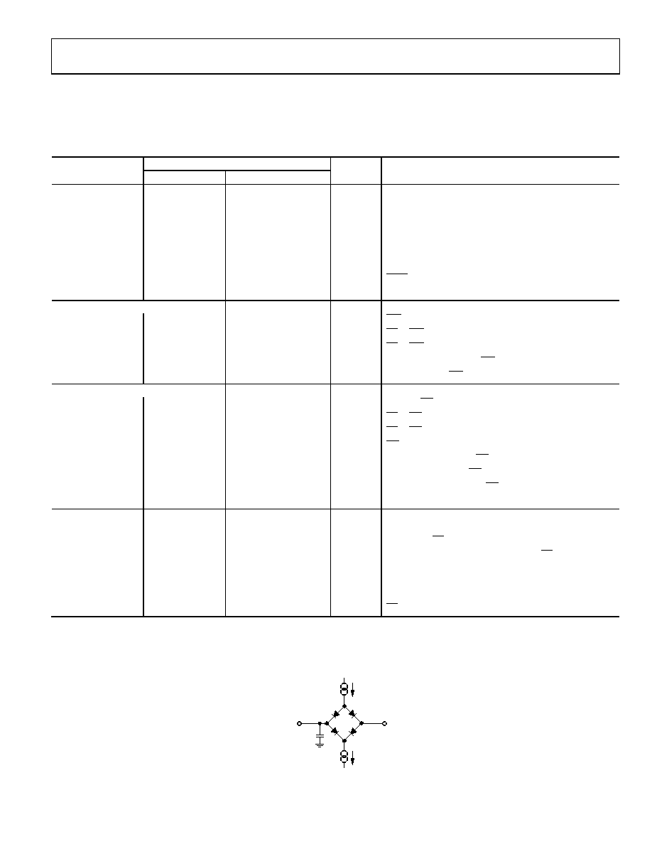
200A
IOL
200A
IOH
1.6V
TO OUTPUT
PIN
CL
25pF
05020-
002
Figure 2. Load Circuit for Digital Output Timing Specification
相关PDF资料 |
PDF描述 |
|---|---|
| AD9218BSTZ-65 | IC ADC 10BIT DUAL 65MSPS 48-LQFP |
| 97-3108B-18-4S | CONN PLUG RT ANG 4POS W/SOCKETS |
| ICL3232EIAZ | IC 2DRVR/2RCVR RS232 3V 16-SSOP |
| VI-BTR-MX-F1 | CONVERTER MOD DC/DC 7.5V 75W |
| ISL3175EIBZ | TXRX ESD 3.3V RS-485/422 8-SOIC |
相关代理商/技术参数 |
参数描述 |
|---|---|
| AD7657YSTZ-1 | 功能描述:IC ADC 14BIT 6CH 250KSPS 64LQFP RoHS:是 类别:集成电路 (IC) >> 数据采集 - 模数转换器 系列:- 标准包装:1,000 系列:- 位数:12 采样率(每秒):300k 数据接口:并联 转换器数目:1 功率耗散(最大):75mW 电压电源:单电源 工作温度:0°C ~ 70°C 安装类型:表面贴装 封装/外壳:24-SOIC(0.295",7.50mm 宽) 供应商设备封装:24-SOIC 包装:带卷 (TR) 输入数目和类型:1 个单端,单极;1 个单端,双极 |
| AD7657YSTZ-1-RL | 功能描述:IC ADC 14BIT 6CH 250KSPS 64LQFP RoHS:是 类别:集成电路 (IC) >> 数据采集 - 模数转换器 系列:- 标准包装:1,000 系列:- 位数:12 采样率(每秒):300k 数据接口:并联 转换器数目:1 功率耗散(最大):75mW 电压电源:单电源 工作温度:0°C ~ 70°C 安装类型:表面贴装 封装/外壳:24-SOIC(0.295",7.50mm 宽) 供应商设备封装:24-SOIC 包装:带卷 (TR) 输入数目和类型:1 个单端,单极;1 个单端,双极 |
| AD7657YSTZ-REEL | 功能描述:IC ADC 14BIT 6CH 250KSPS 64LQFP RoHS:是 类别:集成电路 (IC) >> 数据采集 - 模数转换器 系列:- 标准包装:1,000 系列:- 位数:12 采样率(每秒):300k 数据接口:并联 转换器数目:1 功率耗散(最大):75mW 电压电源:单电源 工作温度:0°C ~ 70°C 安装类型:表面贴装 封装/外壳:24-SOIC(0.295",7.50mm 宽) 供应商设备封装:24-SOIC 包装:带卷 (TR) 输入数目和类型:1 个单端,单极;1 个单端,双极 |
| AD7658 | 制造商:AD 制造商全称:Analog Devices 功能描述:250 kSPS, 6-Channel,Simultaneous Sampling, Bipolar 12/14/16-Bit ADC |
| AD7658-1 | 制造商:AD 制造商全称:Analog Devices 功能描述:250 kSPS, 6-Channel, Simultaneous Sampling, Bipolar, 16-/14-/12-Bit ADC |
发布紧急采购,3分钟左右您将得到回复。