- 您现在的位置:买卖IC网 > PDF目录10664 > AD7663ASTZ (Analog Devices Inc)IC ADC 16BIT CMOS 48-LQFP PDF资料下载
参数资料
| 型号: | AD7663ASTZ |
| 厂商: | Analog Devices Inc |
| 文件页数: | 6/24页 |
| 文件大小: | 0K |
| 描述: | IC ADC 16BIT CMOS 48-LQFP |
| 产品培训模块: | Power Line Monitoring |
| 标准包装: | 1 |
| 系列: | PulSAR® |
| 位数: | 16 |
| 采样率(每秒): | 250k |
| 数据接口: | 串行,并联 |
| 转换器数目: | 1 |
| 功率耗散(最大): | 41mW |
| 电压电源: | 模拟和数字 |
| 工作温度: | -40°C ~ 85°C |
| 安装类型: | 表面贴装 |
| 封装/外壳: | 48-LQFP |
| 供应商设备封装: | 48-LQFP(7x7) |
| 包装: | 托盘 |
| 输入数目和类型: | 4 个单端,单极;4 个单端,双极 |
| 产品目录页面: | 778 (CN2011-ZH PDF) |
| 配用: | EVAL-AD7663CBZ-ND - BOARD EVALUATION FOR AD7663 |
REV. B
AD7663
–14–
75
70
65
60
55
50
45
40
35
0
10
100
1000
CMRR
–
dB
FREQUENCY – kHz
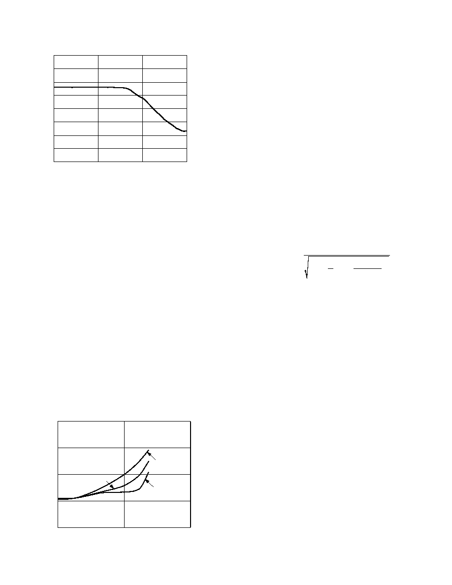
Figure 7. Analog Input CMRR vs. Frequency
During the acquisition phase for ac signals, the AD7663 behaves
like a one-pole RC filter consisting of the equivalent resistance of
the resistive scaler R/2 in series with R1 and CS. The resistor R1
is typically 2700
W and is a lumped component made up of some
serial resistors and the on-resistance of the switches. The capacitor
CS is typically 60 pF and is mainly the ADC sampling capacitor.
This one-pole filter with a typical –3 dB cutoff frequency of
800 kHz reduces undesirable aliasing effects and limits the noise
coming from the inputs.
Except when using the 0 V to 2.5 V analog input voltage range,
the AD7663 has to be driven by a very low impedance source to
avoid gain errors. That can be done by using a driver amplifier
whose choice is eased by the primarily resistive analog input
circuitry of the AD7663.
When using the 0 V to 2.5 V analog input voltage range, the input
impedance of the AD7663 is very high so the AD7663 can be
driven directly by a low impedance source without gain error.
That allows, as shown in Figure 5, putting an external one-pole
RC filter between the output of the amplifier output and the ADC
analog inputs to even further improve the noise filtering by the
AD7663 analog input circuit. However, the source impedance
has to be kept low because it affects the ac performances, especially
the total harmonic distortion (THD). The maximum source
impedance depends on the amount of THD that can be tolerated.
The THD degradation is a function of the source impedance
and the maximum input frequency as shown in Figure 8.
FREQUENCY – kHz
–70
10
THD
100
1000
–80
–90
–100
–110
R = 100
R = 11
R = 50
Figure 8. THD vs. Analog Input Frequency and Input
Resistance (0 V to 2.5 V Only)
Driver Amplifier Choice
Although the AD7663 is easy to drive, the driver amplifier needs
to meet at least the following requirements:
The driver amplifier and the AD7663 analog input circuit
have to be able, together, to settle for a full-scale step of the
capacitor array at a 16-bit level (0.0015%). In the amplifier’s
data sheet, the settling at 0.1% to 0.01% is more commonly
specified. It could significantly differ from the settling time at
16-bit level and, therefore, it should be verified prior to the
driver selection. The tiny op amp AD8021, which combines
ultralow noise and a high gain bandwidth, meets this settling
time requirement even when used with a high gain up to 13.
The noise generated by the driver amplifier needs to be kept
as low as possible in order to preserve the SNR and transition
noise performance of the AD7663. The noise coming from
the driver is first scaled down by the resistive scaler according
to the analog input voltage range used, and is then filtered by
the AD7663 analog input circuit one-pole, low-pass filter
made by (R/2 + R1) and CS. The SNR degradation due to
the amplifier is
SNR
f
Ne
FSR
LOSS
dB
N
=
+
20
28
784
2
25
3
2
log
.
–
p
where:
f–3 dB is the –3 dB input bandwidth in MHz of the AD7663
(0.8 MHz) or the cut-off frequency of the input filter
if any used (0 V to 2.5 V range).
N
is the noise factor of the amplifier (1 if in buffer
configuration).
eN
is the equivalent input noise voltage of the op amp
in nV/Hz
1/2.
FSR is the full-scale span (i.e., 5 V for ±2.5 V range).
For instance, when using the 0 V to 2.5 V range, a driver
like the AD8610 with an equivalent input noise of 6 nV/
÷Hz
and configured as a buffer, thus with a noise gain of 1, the
SNR degrades by only 0.24 dB.
The driver needs to have a THD performance suitable to
that of the AD7663. TPC 10 gives the THD versus frequency
that the driver should preferably exceed.
The AD8021 meets these requirements and is usually appropri-
ate for almost all applications. The AD8021 needs an external
compensation capacitor of 10 pF. This capacitor should have good
linearity as an NPO ceramic or mica type.
The AD8022 could also be used where a dual version is needed
and gain of 1 is used.
The AD829 is another alternative where high frequency (above
100 kHz) performance is not required. In a gain of 1, it requires
an 82 pF compensation capacitor.
The AD8610 is also another option where low bias current is
needed in low frequency applications.
相关PDF资料 |
PDF描述 |
|---|---|
| VI-21N-MX | CONVERTER MOD DC/DC 18.5V 75W |
| AD9243ASZ | IC ADC 14BIT 3MSPS 44-MQFP |
| AD7893ANZ-2 | IC ADC 12BIT SRL T/H LP 8-DIP |
| MAX9034AUD+T | IC COMPARATOR QUAD 14-TSSOP |
| MAX9039BEBT+T | IC COMPARATOR SNGL 6-UCSP |
相关代理商/技术参数 |
参数描述 |
|---|---|
| AD7663ASTZ | 制造商:Analog Devices 功能描述:IC, ADC, 16BIT, 250KSPS, LQFP-48 |
| AD7663ASTZRL | 功能描述:IC ADC 16BIT CMOS 48-LQFP T/R RoHS:是 类别:集成电路 (IC) >> 数据采集 - 模数转换器 系列:PulSAR® 标准包装:1,000 系列:- 位数:12 采样率(每秒):300k 数据接口:并联 转换器数目:1 功率耗散(最大):75mW 电压电源:单电源 工作温度:0°C ~ 70°C 安装类型:表面贴装 封装/外壳:24-SOIC(0.295",7.50mm 宽) 供应商设备封装:24-SOIC 包装:带卷 (TR) 输入数目和类型:1 个单端,单极;1 个单端,双极 |
| AD7663CB1 | 制造商:AD 制造商全称:Analog Devices 功能描述:16-Bit, 250 kSPS CMOS ADC |
| AD7664 | 制造商:AD 制造商全称:Analog Devices 功能描述:16-Bit, 570 kSPS CMOS ADC |
| AD7664ACP | 制造商:Analog Devices 功能描述:ADC Single SAR 570ksps 16-bit Parallel/Serial 48-Pin LFCSP EP 制造商:Analog Devices 功能描述:ADC SGL SAR 570KSPS 16BIT PARALLEL/SERL 48LFCSP EP - Trays 制造商:Rochester Electronics LLC 功能描述:16-BIT, 500KSPS CMOS ADC - Bulk |
发布紧急采购,3分钟左右您将得到回复。