- 您现在的位置:买卖IC网 > PDF目录11767 > AD7669JPZ (Analog Devices Inc)IC I/O PORT 8BIT ANLG 28-PLCC PDF资料下载
参数资料
| 型号: | AD7669JPZ |
| 厂商: | Analog Devices Inc |
| 文件页数: | 14/20页 |
| 文件大小: | 0K |
| 描述: | IC I/O PORT 8BIT ANLG 28-PLCC |
| 标准包装: | 1 |
| 系列: | LC²MOS |
| 应用: | 模拟 I/O |
| 接口: | 总线 |
| 电源电压: | 4.75 V ~ 5.25 V |
| 封装/外壳: | 28-LCC(J 形引线) |
| 供应商设备封装: | 28-PLCC(11.51x11.51) |
| 包装: | 管件 |
| 安装类型: | 表面贴装 |
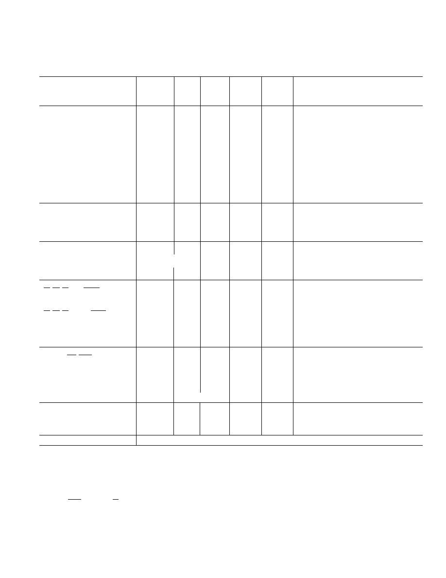
ADC SPECIFICATIONS
AD7569
J, A Versions
3
AD7569
AD7669
K, B
AD7569
Parameter
J Version
Versions
S Version
T Version
Units
Conditions/Comments
DC ACCURACY
Resolution
3
8
Bits
Total Unadjusted Error
4
±3
±4
LSB typ
Relative Accuracy
4
±1
±1/2
±1
±1/2
LSB max
Differential Nonlinearity
4
±1
±3/4
±1
±3/4
LSB max
No Missing Codes
Unipolar Offset Error
Typical tempco is 10
V/°C for +1.25 V range; V
SS = 0 V
@ +25
°C
±2
± 1.5
±2
± 1.5
LSB max
TMIN to TMAX
±3
± 2.5
±3
± 2.5
LSB max
Bipolar Zero Offset Error
Typical tempco is 20
V/°C for + 1.25 V range; V
SS = –5 V
@ +25
°C
±3
± 2.5
±3
± 2.5
LSB max
TMIN to TMAX
± 3.5
±3
±4
± 3.5
LSB max
Full-Scale Error
5
VDD = 5 V
@ +25
°C
–4, +0
LSB max
TMIN to TMAX
–5.5, +1.5
–7.5, +2
LSB max
Full Scale/V
DD, TA = +25°C
0.5
LSB max
VIN = +2.5 V; VDD = ± 5%
Full Scale/V
SS, TA = +25°C
0.5
LSB max
VIN = –2.5 V; VSS = ± 5%
DYNAMIC PERFORMANCE
Signal-to-Noise Ratio
4 (SNR)
44
46
44
45
dB min
VIN = 100 kHz full-scale sine wave with fSAMPLING = 400 kHz
6
Total Harmonic Distortion
4 (THD)
48
dB max
VIN = 100 kHz full-scale sine wave with fSAMPLING = 400 kHz
6
Intermodulation Distortion
4 (IMD)
60
dB typ
fa = 99 kHz, fb = 96.7 kHz with fSAMPLING = 400 kHz
Frequency Response
0.1
dB typ
VIN = ± 2.5 V, dc to 200 kHz sine wave
Track/Hold Acquisition Time
7
200
300
ns typ
ANALOG INPUT
Input Voltage Ranges
Unipolar
0 to +1.25/ +2.5
Volts
VDD = +5 V; VSS = 0 V
Bipolar
±1.25/±2.5
Volts
VDD = +5 V; VSS = –5 V
Input Current
±300
A max
See equivalent circuit Figure 5
Input Capacitance
10
pF typ
LOGIC INPUTS
CS
, RD, ST, CLK, RESET, RANGE
Input Low Voltage, VINL
0.8
V max
Input High Voltage, VINH
2.4
V min
Input Capacitance
8
10
pF max
CS
, RD, ST, RANGE, RESET
Input Leakage Current
10
A max
V IN = 0 to VDD
CLK
Input Current
IINL
–1.6
mA max
VIN = 0 V
IINH
40
A max
VIN = VDD
LOGIC OUTPUTS
DB0–DB7, INT, BUSY
VOL, Output Low Voltage
0.4
V max
ISINK = 1.6 mA
VOH, Output High Voltage
4.0
V min
ISOURCE = 200 A
DB0–DB7
Floating State Leakage Current
10
A max
Floating State Output Capacitance
8
10
pF max
Output Coding (Single Supply)
Binary
Output Coding (Dual Supply)
2s Complement
CONVERSION TIME
With External Clock
2
s max
fCLK = 5 MHz
With Internal Clock, TA = +25°C
1.6
s min
Using recommended clock components shown in Figure 21.
2.6
s max
Clock frequency can be adjusted by varying RCLK.
POWER REQUIREMENTS
As per DAC Specifications
NOTES
1
Except where noted, specifications apply for all ranges including bipolar ranges with dual supply operation.
2Temperature ranges are as follows: J, K versions; 0
°C to +70°C
A, B versions; –40
°C to +85°C
S, T versions; –55
°C to +125°C
31 LSB = 4.88 mV for 0 V to +1.25 V range, 9.76 mV for 0 V to +2.5 V and
±1.25 V ranges and 19.5 mV for +2.5 V range.
4See Terminology.
5Includes internal voltage reference error and is calculated after offset error has been adjusted out. Ideal unipolar last code transition occurs at (FS – 3/2 LSB). Ideal bipolar last code transition occurs at
(FS/2 – 3/2 LSB).
6Exact frequencies are 101 kHz and 384 kHz to avoid harmonics coinciding with sampling frequency.
7Rising edge of BUSY to falling edge of ST. The time given refers to the acquisition time, which gives a 3 dB degradation in SNR from the tested figure.
8Sample tested at +25
°C to ensure compliance.
Specifications subject to change without notice.
(VDD = +5 V
5%; VSS
1 = RANGE = AGND
DAC = AGNDDAC = DGND = 0 V; fCLK = 5 MHz external unless other-
wise noted. All specifications TMIN to TMAX unless otherwise noted.) Specifications apply to Mode 1 interface.
AD7569/AD7669
–3–
REV. B
相关PDF资料 |
PDF描述 |
|---|---|
| D38999/20JC4PN | CONN RCPT 4POS WALL MNT W/PINS |
| MS27497E18A66P | CONN RCPT 66POS WALL MNT W/PINS |
| AD7569AQ | IC I/O PORT 8BIT ANLG 24-CDIP |
| D38999/20WD97PN | CONN RCPT 12POS WALL MNT W/PINS |
| AD6620ASZ-REEL | IC DGTL RCVR DUAL 67MSPS 80-PQFP |
相关代理商/技术参数 |
参数描述 |
|---|---|
| AD7669JR | 制造商:Analog Devices 功能描述:Data Acquisition System Single ADC Dual DAC 8-Bit 28-Pin SOIC W 制造商:Rochester Electronics LLC 功能描述:COMPLETE 8-BIT 1/O SYSTEM - Bulk |
| AD7669JR-REEL | 制造商:Rochester Electronics LLC 功能描述:- Tape and Reel |
| AD7669JRZ | 功能描述:IC I/O PORT 8BIT ANLG 28SOIC RoHS:是 类别:集成电路 (IC) >> 接口 - 专用 系列:LC²MOS 特色产品:NXP - I2C Interface 标准包装:1 系列:- 应用:2 通道 I²C 多路复用器 接口:I²C,SM 总线 电源电压:2.3 V ~ 5.5 V 封装/外壳:16-TSSOP(0.173",4.40mm 宽) 供应商设备封装:16-TSSOP 包装:剪切带 (CT) 安装类型:表面贴装 产品目录页面:825 (CN2011-ZH PDF) 其它名称:568-1854-1 |
| AD7669JRZ-REEL | 功能描述:IC I/O PORT 8BIT ANLG 28SOIC RoHS:是 类别:集成电路 (IC) >> 接口 - 专用 系列:LC²MOS 特色产品:NXP - I2C Interface 标准包装:1 系列:- 应用:2 通道 I²C 多路复用器 接口:I²C,SM 总线 电源电压:2.3 V ~ 5.5 V 封装/外壳:16-TSSOP(0.173",4.40mm 宽) 供应商设备封装:16-TSSOP 包装:剪切带 (CT) 安装类型:表面贴装 产品目录页面:825 (CN2011-ZH PDF) 其它名称:568-1854-1 |
| AD766AN | 功能描述:IC DAC 16BIT W/REF DSP 16-DIP RoHS:否 类别:集成电路 (IC) >> 数据采集 - 数模转换器 系列:DACPORT® 产品培训模块:Data Converter Fundamentals DAC Architectures 标准包装:750 系列:- 设置时间:7µs 位数:16 数据接口:并联 转换器数目:1 电压电源:双 ± 功率耗散(最大):100mW 工作温度:0°C ~ 70°C 安装类型:表面贴装 封装/外壳:28-LCC(J 形引线) 供应商设备封装:28-PLCC(11.51x11.51) 包装:带卷 (TR) 输出数目和类型:1 电压,单极;1 电压,双极 采样率(每秒):143k |
发布紧急采购,3分钟左右您将得到回复。