- 您现在的位置:买卖IC网 > PDF目录11767 > AD7669JRZ-REEL (Analog Devices Inc)IC I/O PORT 8BIT ANLG 28SOIC PDF资料下载
参数资料
| 型号: | AD7669JRZ-REEL |
| 厂商: | Analog Devices Inc |
| 文件页数: | 10/20页 |
| 文件大小: | 0K |
| 描述: | IC I/O PORT 8BIT ANLG 28SOIC |
| 标准包装: | 1,000 |
| 系列: | LC²MOS |
| 应用: | 模拟 I/O |
| 接口: | 总线 |
| 电源电压: | 4.75 V ~ 5.25 V |
| 封装/外壳: | 28-SOIC(0.295",7.50mm 宽) |
| 供应商设备封装: | 28-SOIC W |
| 包装: | 带卷 (TR) |
| 安装类型: | 表面贴装 |
–18–
REV. B
AD7569/AD7669
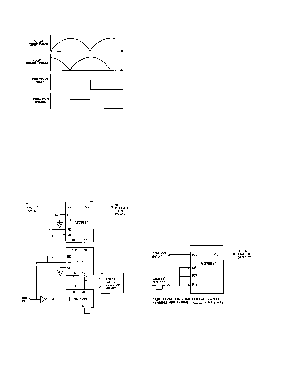
Figure 27. Typical DAC Output Voltages for Microstepping
and Direction Signals for Clockwise Rotation with the
UDN-2998W
ANALOG DELAY LINE—AD7569
In many applications, especially in audio systems, it is necessary
to provide a delay on the input signal. The circuit of Figure 28
shows how a simple analog delay line can be implemented,
based on the AD7569. The input signal is sampled using the
AD7569 ADC, and converted data is loaded into the 6116 (2K
8 static ram). The inverted input clock drives a counter that
selects the address for the 6116. The delay is selected by choos-
ing one of the output lines of the HCT4040 counter to reset the
coun-ter. This can be done using a simple switch in a manual
system or by a multiplexer in a programmable delay application.
Data is written to the DAC using the inverted input clock signal.
Figure 28. Analog Delay Line
On initial start-up, the output voltage, VO, will be invalid until
the length of the delay is reached (i.e., until the counter is re-
set). From this point forward, the delayed data is read from the
6116 and loaded to the DAC before the newly converted data is
written into the same memory location. The input clock to the
system can be a square wave of maximum input frequency 200
kHz
(assuming 2
s conversion time for the ADC). The mark/space
ratio of the input clock can be varied to maximize the sampling
frequency if required. The clock low time has to be equal to the
conversion time and access time of the ADC plus the setup time
required for the 6116. The clock high time has only to be equal
to the setup time for the DAC plus the delay time through the
counter and the access time of the 6116.
The amount of memory used, as well as the sampling frequency,
determines the maximum possible delay. Using the HCT4040,
and the 6116 with an input clock frequency of 200 kHz, the
maximum delay is 5 ms on a maximum input frequency of
100 kHz. Using 64K memory, with an 8 kHz input clock fre-
quency, the maximum delay is 8 seconds on a maximum input
frequency of 4 kHz.
TRANSIENT RECORDER—AD7569
The scheme just outlined can also form the basis for a transient
recorder. In this case, transients on the input signal are con-
verted and stored in memory. The transient can then be recalled
from memory at a later time, and the transient waveform can be
recreated using the AD7569 DAC.
INFINITE SAMPLE-AND-HOLD—AD7569
The AD7569 is ideal for implementing a single-chip infinite
sample-and-hold function. Basically, the ADC samples and con-
verts the input signal into an 8-bit digital word. The 8 bits of
data are then loaded to the DAC and the sampled value is re-
stored to analog form. The sampled value is held until the DAC
register is updated. The full-scale matching between the ADC
and the DAC on the AD7569 ensures a typical error of less than
1% between the analog input voltage and the “held” output
voltage. Figure 29 shows the connections required on the
AD7569 to achieve this infinite sample-and-hold function.
Figure 29. Infinite Sample-and-Hold
相关PDF资料 |
PDF描述 |
|---|---|
| 5413515-8 | CONN JACK BNC RT ANG 50 OHM 30AU |
| AD7669ARZ-REEL | IC I/O PORT 8BIT ANALOG 28SOIC |
| PIC16C505-04I/P | IC MCU OTP 1KX12 14DIP |
| VI-B44-IW-F3 | CONVERTER MOD DC/DC 48V 100W |
| VI-B42-IW-F4 | CONVERTER MOD DC/DC 15V 100W |
相关代理商/技术参数 |
参数描述 |
|---|---|
| AD766AN | 功能描述:IC DAC 16BIT W/REF DSP 16-DIP RoHS:否 类别:集成电路 (IC) >> 数据采集 - 数模转换器 系列:DACPORT® 产品培训模块:Data Converter Fundamentals DAC Architectures 标准包装:750 系列:- 设置时间:7µs 位数:16 数据接口:并联 转换器数目:1 电压电源:双 ± 功率耗散(最大):100mW 工作温度:0°C ~ 70°C 安装类型:表面贴装 封装/外壳:28-LCC(J 形引线) 供应商设备封装:28-PLCC(11.51x11.51) 包装:带卷 (TR) 输出数目和类型:1 电压,单极;1 电压,双极 采样率(每秒):143k |
| AD766ANZ | 功能描述:IC DAC 16BIT W/REF DSP 16-DIP RoHS:是 类别:集成电路 (IC) >> 数据采集 - 数模转换器 系列:DACPORT® 标准包装:1 系列:- 设置时间:4.5µs 位数:12 数据接口:串行,SPI? 转换器数目:1 电压电源:单电源 功率耗散(最大):- 工作温度:-40°C ~ 125°C 安装类型:表面贴装 封装/外壳:8-SOIC(0.154",3.90mm 宽) 供应商设备封装:8-SOICN 包装:剪切带 (CT) 输出数目和类型:1 电压,单极;1 电压,双极 采样率(每秒):* 其它名称:MCP4921T-E/SNCTMCP4921T-E/SNRCTMCP4921T-E/SNRCT-ND |
| AD766JN | 功能描述:IC DAC 16BIT W/VREF 16-DIP RoHS:否 类别:集成电路 (IC) >> 数据采集 - 数模转换器 系列:DACPORT® 产品培训模块:Data Converter Fundamentals DAC Architectures 标准包装:750 系列:- 设置时间:7µs 位数:16 数据接口:并联 转换器数目:1 电压电源:双 ± 功率耗散(最大):100mW 工作温度:0°C ~ 70°C 安装类型:表面贴装 封装/外壳:28-LCC(J 形引线) 供应商设备封装:28-PLCC(11.51x11.51) 包装:带卷 (TR) 输出数目和类型:1 电压,单极;1 电压,双极 采样率(每秒):143k |
| AD766JNZ | 功能描述:IC DAC 16BIT W/VREF 16-DIP RoHS:是 类别:集成电路 (IC) >> 数据采集 - 数模转换器 系列:DACPORT® 标准包装:1 系列:- 设置时间:4.5µs 位数:12 数据接口:串行,SPI? 转换器数目:1 电压电源:单电源 功率耗散(最大):- 工作温度:-40°C ~ 125°C 安装类型:表面贴装 封装/外壳:8-SOIC(0.154",3.90mm 宽) 供应商设备封装:8-SOICN 包装:剪切带 (CT) 输出数目和类型:1 电压,单极;1 电压,双极 采样率(每秒):* 其它名称:MCP4921T-E/SNCTMCP4921T-E/SNRCTMCP4921T-E/SNRCT-ND |
| AD766SD/883B | 功能描述:数模转换器- DAC 16-BIT DSP DAC IC RoHS:否 制造商:Texas Instruments 转换器数量:1 DAC 输出端数量:1 转换速率:2 MSPs 分辨率:16 bit 接口类型:QSPI, SPI, Serial (3-Wire, Microwire) 稳定时间:1 us 最大工作温度:+ 85 C 安装风格:SMD/SMT 封装 / 箱体:SOIC-14 封装:Tube |
发布紧急采购,3分钟左右您将得到回复。