- 您现在的位置:买卖IC网 > PDF目录11767 > AD7669JRZ (Analog Devices Inc)IC I/O PORT 8BIT ANLG 28SOIC PDF资料下载
参数资料
| 型号: | AD7669JRZ |
| 厂商: | Analog Devices Inc |
| 文件页数: | 20/20页 |
| 文件大小: | 0K |
| 描述: | IC I/O PORT 8BIT ANLG 28SOIC |
| 标准包装: | 27 |
| 系列: | LC²MOS |
| 应用: | 模拟 I/O |
| 接口: | 总线 |
| 电源电压: | 4.75 V ~ 5.25 V |
| 封装/外壳: | 28-SOIC(0.295",7.50mm 宽) |
| 供应商设备封装: | 28-SOIC W |
| 包装: | 管件 |
| 安装类型: | 表面贴装 |
AD7569/AD7669
–9–
REV. B
CIRCUIT DESCRIPTION
D/A SECTION
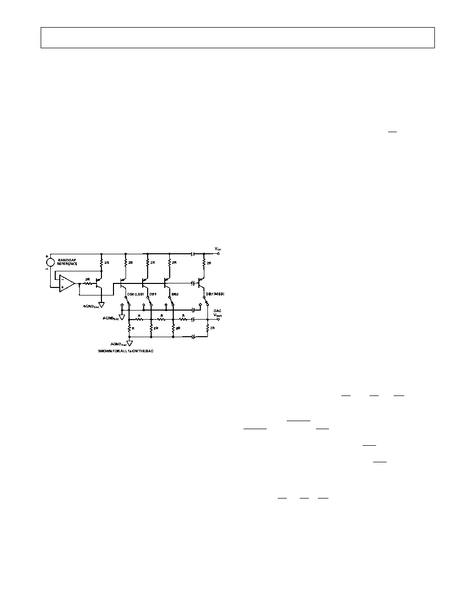
The AD7569 contains an 8-bit, voltage-mode, D/A converter
that uses eight equally weighted current sources switched into
an R-2R ladder network to give a direct but unbuffered 0 V to
+1.25 V output range. The AD7669 is similar, but contains two
D/A converters. The current sources are fabricated using PNP
transistors. These transistors allow current sources that are
driven from positive voltage logic and give a zero-based output
range. The output voltage from the voltage switching R-2R lad-
der network has the same positive polarity as the reference;
therefore, the D/A converter can be operated from a single
power supply rail.
The PNP current sources are generated using the on-chip
bandgap reference and a control amplifier. The current sources
are switched to either the ladder or AGNDDAC by high speed
p-channel switches. These high-speed switches ensure a fast set-
tling time for the output voltage of the DAC. The R-2R ladder
network of the DAC consists of highly stable, thin-film resistors.
A simplified circuit diagram for the D/A converter section is
shown in Figure 3. An identical D/A converter is used as part of
the A/D converter, which is discussed later.
Figure 3. DAC Simplified Circuit Diagram
OP AMP SECTION
The output from the D/A converter is buffered by a high speed,
noninverting op amp. This op amp is capable of developing
±2.5 V across a 2 k and 100 pF load to AGND
DAC. The am-
plifier can be operated from a single +5 V supply to give two
unipolar output ranges, or from dual supplies (
±5 V) to allow
two bipolar output ranges.
The feedback path of the amplifier contains a gain/offset net-
work that provides four voltage ranges at the output of the op
amp. The output voltage range is determined by the RANGE
and VSS inputs. (See Table I in the Pin Function Description
section.) The four possible output ranges are: 0 V to +1.25 V,
0 V to +2.5 V,
±1.25 V and ±2.5 V. It should be noted that
whichever range is selected for the output amplifier also applies
to the input voltage range of the A/D converter.
The output amplifier settles to within 1/2 LSB of its final value
in typically less than 500 ns. Operating the part from single or
dual supplies has no effect on the positive-going settling time.
However, the negative-going output settling time to voltages
near 0 V in single supply will be slightly longer than the settling
time to negative full scale for dual supply operation. Addition-
ally, to ensure that the output voltage can go to 0 V in single
supply, a transistor on the output acts as a passive pull-down
with output voltages near 0 V with VSS = 0 V. This means that
the sink capability of the amplifier is reduced as the output volt-
age nears 0 V in single supply. In dual supply operation the full
sink capability of 1.25 mA is maintained over the entire output
voltage range.
For all other parameters, the single and dual supply perfor-
mances of the amplifier are essentially identical. The output
noise from the amplifier, with full scale on the DAC, is 200
V
peak-to-peak. The spot noise at 1 kHz is 35 nV/
√Hz with all 0s
on the DAC. A noise spectral density versus frequency plot for
the amplifier is shown in the typical performance graphs.
VOLTAGE REFERENCE
The AD7569/AD7669 contains an on-chip bandgap reference
that provides a low noise, temperature compensated reference
voltage for both the DAC and the ADC. The reference is
trimmed for absolute accuracy and temperature coefficient. The
bandgap reference is generated with respect to VDD. It is buff-
ered by a separate control amplifier for both the DAC and the
ADC reference. This can be seen in the DAC ladder network
configuration in Figure 3.
DIGITAL SECTION
The data pins on the AD7569/AD7669 provide a connection
between the external bus and DAC data inputs and ADC data
outputs. The threshold levels of all digital inputs and outputs
are compatible with either TTL or 5 V CMOS levels. Internal
input protection of all digital pins is achieved by on-chip distrib-
uted diodes.
The data format is straight binary when the part is used in single
supply (VSS = 0 V). However, when a VSS of –5 V is applied, the
data format becomes twos complement. This data format ap-
plies to the digital inputs of the DAC and the digital outputs of
the ADC.
ADC SECTION
The analog-to-digital converter on the AD7569/AD7669 uses
the successive approximation technique to achieve a fast conver-
sion time of 2
s and provides an 8-bit parallel digital output.
The reference for the ADC is provided by the on-chip bandgap
reference.
Conversion start is controlled by ST or by CS and RD. Once a
conversion has been started, another conversion start should not
be attempted until the conversion in progress is completed.
Exercising the RESET input does not affect conversion; the
RESET
input resets the INT line high, which is useful in inter-
rupt driven systems where a READ has not been performed at
the end of the previous conversion. The INT line does not have
to be cleared at the end of conversion. The ADC will continue
to convert correctly, but the function of the INT line will be
affected.
Figure 4 shows the operating waveforms for a conversion cycle.
The analog input voltage, VIN, is held 50 ns typical after the fall-
ing edge of ST or (CS & RD). The MSB decision is made ap-
proximately 50 ns after the second falling edge of the input
CLK following a conversion start. If t1 in Figure 4 is greater
than 50 ns, then the falling edge of the input CLK will be seen
as the first falling clock edge. If t1 is less than 50 ns, the first fall-
ing clock edge of the conversion will not occur until one clock
cycle later. The succeeding bit decisions are made approxi-
mately 50 ns after a CLK edge until conversion is complete.
相关PDF资料 |
PDF描述 |
|---|---|
| AD7569BRZ | IC I/O PORT 8BIT ANALOG 24SOIC |
| PIC16F723A-I/SP | MCU PIC 7KB FLASH XLP 28-SPDIP |
| PIC16C505-04/SL | IC MCU OTP 1KX12 14SOIC |
| PIC16LF1825-I/P | MCU PIC 14KB FLASH 14-DIP |
| PIC16LF1826-I/MV | IC MCU 8BIT FLASH 28UQFN |
相关代理商/技术参数 |
参数描述 |
|---|---|
| AD7669JRZ-REEL | 功能描述:IC I/O PORT 8BIT ANLG 28SOIC RoHS:是 类别:集成电路 (IC) >> 接口 - 专用 系列:LC²MOS 特色产品:NXP - I2C Interface 标准包装:1 系列:- 应用:2 通道 I²C 多路复用器 接口:I²C,SM 总线 电源电压:2.3 V ~ 5.5 V 封装/外壳:16-TSSOP(0.173",4.40mm 宽) 供应商设备封装:16-TSSOP 包装:剪切带 (CT) 安装类型:表面贴装 产品目录页面:825 (CN2011-ZH PDF) 其它名称:568-1854-1 |
| AD766AN | 功能描述:IC DAC 16BIT W/REF DSP 16-DIP RoHS:否 类别:集成电路 (IC) >> 数据采集 - 数模转换器 系列:DACPORT® 产品培训模块:Data Converter Fundamentals DAC Architectures 标准包装:750 系列:- 设置时间:7µs 位数:16 数据接口:并联 转换器数目:1 电压电源:双 ± 功率耗散(最大):100mW 工作温度:0°C ~ 70°C 安装类型:表面贴装 封装/外壳:28-LCC(J 形引线) 供应商设备封装:28-PLCC(11.51x11.51) 包装:带卷 (TR) 输出数目和类型:1 电压,单极;1 电压,双极 采样率(每秒):143k |
| AD766ANZ | 功能描述:IC DAC 16BIT W/REF DSP 16-DIP RoHS:是 类别:集成电路 (IC) >> 数据采集 - 数模转换器 系列:DACPORT® 标准包装:1 系列:- 设置时间:4.5µs 位数:12 数据接口:串行,SPI? 转换器数目:1 电压电源:单电源 功率耗散(最大):- 工作温度:-40°C ~ 125°C 安装类型:表面贴装 封装/外壳:8-SOIC(0.154",3.90mm 宽) 供应商设备封装:8-SOICN 包装:剪切带 (CT) 输出数目和类型:1 电压,单极;1 电压,双极 采样率(每秒):* 其它名称:MCP4921T-E/SNCTMCP4921T-E/SNRCTMCP4921T-E/SNRCT-ND |
| AD766JN | 功能描述:IC DAC 16BIT W/VREF 16-DIP RoHS:否 类别:集成电路 (IC) >> 数据采集 - 数模转换器 系列:DACPORT® 产品培训模块:Data Converter Fundamentals DAC Architectures 标准包装:750 系列:- 设置时间:7µs 位数:16 数据接口:并联 转换器数目:1 电压电源:双 ± 功率耗散(最大):100mW 工作温度:0°C ~ 70°C 安装类型:表面贴装 封装/外壳:28-LCC(J 形引线) 供应商设备封装:28-PLCC(11.51x11.51) 包装:带卷 (TR) 输出数目和类型:1 电压,单极;1 电压,双极 采样率(每秒):143k |
| AD766JNZ | 功能描述:IC DAC 16BIT W/VREF 16-DIP RoHS:是 类别:集成电路 (IC) >> 数据采集 - 数模转换器 系列:DACPORT® 标准包装:1 系列:- 设置时间:4.5µs 位数:12 数据接口:串行,SPI? 转换器数目:1 电压电源:单电源 功率耗散(最大):- 工作温度:-40°C ~ 125°C 安装类型:表面贴装 封装/外壳:8-SOIC(0.154",3.90mm 宽) 供应商设备封装:8-SOICN 包装:剪切带 (CT) 输出数目和类型:1 电压,单极;1 电压,双极 采样率(每秒):* 其它名称:MCP4921T-E/SNCTMCP4921T-E/SNRCTMCP4921T-E/SNRCT-ND |
发布紧急采购,3分钟左右您将得到回复。