- 您现在的位置:买卖IC网 > PDF目录10201 > AD7675ASTZRL (Analog Devices Inc)IC ADC 16BIT DIFF INP 48LQFP PDF资料下载
参数资料
| 型号: | AD7675ASTZRL |
| 厂商: | Analog Devices Inc |
| 文件页数: | 6/20页 |
| 文件大小: | 0K |
| 描述: | IC ADC 16BIT DIFF INP 48LQFP |
| 标准包装: | 2,000 |
| 系列: | PulSAR® |
| 位数: | 16 |
| 采样率(每秒): | 100k |
| 数据接口: | 串行,并联 |
| 转换器数目: | 1 |
| 功率耗散(最大): | 25mW |
| 电压电源: | 模拟和数字 |
| 工作温度: | -40°C ~ 85°C |
| 安装类型: | 表面贴装 |
| 封装/外壳: | 48-LQFP |
| 供应商设备封装: | 48-LQFP(7x7) |
| 包装: | 带卷 (TR) |
| 输入数目和类型: | 1 个差分,双极 |
| 配用: | EVAL-AD7675CBZ-ND - BOARD EVALUATION FOR AD7675 |
REV. A
AD7675
–14–
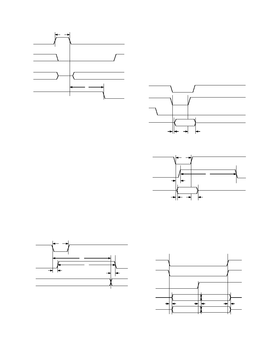
t9
RESET
DATA
BUSY
CNVST
t8
Figure 12. RESET Timing
For other applications, conversions can be automatically initi-
ated. If
CNVST is held low when BUSY is low, the AD7675
controls the acquisition phase and then automatically initiates a
new conversion. By keeping
CNVST low, the AD7675 keeps
the conversion process running by itself. It should be noted that
the analog input has to be settled when BUSY goes low. Also, at
power-up,
CNVST should be brought low once to initiate the
conversion process. In this mode, the AD7675 could sometimes
run slightly faster than the guaranteed limit of 100 kSPS.
DIGITAL INTERFACE
The AD7675 has a versatile digital interface; it can be interfaced
with the host system by using either a serial or parallel interface.
The serial interface is multiplexed on the parallel data bus. The
AD7675 digital interface also accommodates both 3 V or 5 V
logic by simply connecting the OVDD supply pin of the AD7675
to the host system interface digital supply. Finally, by using the
OB/
2C input pin, either two’s complement or straight binary
coding can be used.
The two signals
CS and RD control the interface. When at least
one of these signals is high, the interface outputs are in high
impedance. Usually,
CS allows the selection of each AD7675 in
multicircuits applications and is held low in a single AD7675
design.
RD is generally used to enable the conversion result on
the data bus.
CNVST
BUSY
DATA
BUS
CS = RD = 0
PREVIOUS CONVERSION DATA
NEW DATA
t1
t10
t4
t3
t11
Figure 13. Master Parallel Data Timing for Reading
(Continuous Read)
PARALLEL INTERFACE
The AD7675 is configured to use the parallel interface (Figure 13)
when the SER/
PAR is held low. The data can be read either
after each conversion, which is during the next acquisition
phase, or during the following conversion as shown, respectively,
in Figure 14 and Figure 15. When the data is read during the
conversion, however, it is recommended that it be read-only
during the first half of the conversion phase. That avoids any
potential feedthrough between voltage transients on the digital
interface and the most critical analog conversion circuitry.
DATA
BUS
t12
t13
BUSY
CS
RD
CURRENT
CONVERSION
Figure 14. Slave Parallel Data Timing for Reading
(Read after Convert)
CS = 0
CNVST,
RD
t1
PREVIOUS
CONVERSION
DATA
BUS
t12
t13
BUSY
t4
t3
Figure 15. Slave Parallel Data Timing for Reading (Read
During Convert)
The BYTESWAP pin allows a glueless interface to an 8-bit bus.
As shown in Figure 16, the LSB byte is output on D[7:0] and
the MSB is output on D[15:8] when BYTESWAP is low. When
BYTESWAP is high, the LSB and MSB bytes are swapped and
the LSB is output on D[15:8] and the MSB is output on D[7:0].
By connecting BYTESWAP to an address line, the 16-bit data
can be read in two bytes on either D[15:8] or D[7:0].
CS
RD
BYTE
PINS D[15:8]
PINS D[7:0]
HI-Z
HIGH BYTE
LOW BYTE
HIGH BYTE
HI-Z
t12
t13
Figure 16. 8-Bit Parallel Interface
相关PDF资料 |
PDF描述 |
|---|---|
| MS27474T14F35SC | CONN RCPT 37POS JAM NUT W/SCKT |
| AD7663ACPZRL | IC ADC 16BIT CMOS 5V 48LFCSP |
| VE-263-IW-S | CONVERTER MOD DC/DC 24V 100W |
| AD7663ASTZRL | IC ADC 16BIT CMOS 48-LQFP T/R |
| ADN4692EBRZ-RL7 | IC TXRX MLVDS 100MBPS 8SOIC |
相关代理商/技术参数 |
参数描述 |
|---|---|
| AD7676 | 制造商:AD 制造商全称:Analog Devices 功能描述:16-Bit +-1 LSB INL, 500 kSPS, Differential ADC |
| AD7676ACP | 制造商:Analog Devices 功能描述:ADC SGL SAR 500KSPS 16BIT PARALLEL/SERL 48LFCSP - Trays |
| AD7676ACPRL | 制造商:Analog Devices 功能描述:ADC Single SAR 500ksps 16-bit Parallel/Serial 48-Pin LFCSP EP T/R |
| AD7676ACPZ | 制造商:Rochester Electronics LLC 功能描述: 制造商:Analog Devices 功能描述: |
| AD7676ACPZRL | 制造商:Analog Devices 功能描述:ADC Single SAR 500ksps 16-bit Parallel/Serial 48-Pin LFCSP EP T/R 制造商:Analog Devices 功能描述:ADC SGL SAR 500KSPS 16BIT PARALLEL/SERL 48LFCSP - Tape and Reel |
发布紧急采购,3分钟左右您将得到回复。