参数资料
| 型号: | AD767KPZ |
| 厂商: | Analog Devices Inc |
| 文件页数: | 4/8页 |
| 文件大小: | 0K |
| 描述: | IC DAC 12BIT W/AMP 28-PLCC |
| 产品培训模块: | Data Converter Fundamentals DAC Architectures |
| 标准包装: | 1 |
| 设置时间: | 3µs |
| 位数: | 12 |
| 数据接口: | 并联 |
| 转换器数目: | 1 |
| 电压电源: | 双 ± |
| 工作温度: | 0°C ~ 70°C |
| 安装类型: | 表面贴装 |
| 封装/外壳: | 28-LCC(J 形引线) |
| 供应商设备封装: | 28-PLCC(11.51x11.51) |
| 包装: | 管件 |
| 输出数目和类型: | 1 电压,单极;1 电压,双极 |
| 采样率(每秒): | * |
AD767
REV. A
–4–
THE AD767 OFFERS TRUE 12-BIT PERFORMANCE
OVER THE FULL TEMPERATURE RANGE
LINEARITY ERROR: Analog Devices defines linearity error as
the maximum deviation of the actual, adjusted DAC output
from the ideal analog output (a straight line drawn from 0 to
F.S. – 1 LSB) for any bit combination. This is also referred to as
relative accuracy. The AD767 is laser trimmed to typically
maintain linearity errors at less than
±1/8 LSB for the K and B
versions and
±1/2 LSB for the J, A and S versions. Linearity
over temperature is also held to
±1/2 LSB (K/B) or ±1 LSB
(J/A/S).
MONOTONICITY: A DAC is said to be monotonic if the
output either increases or remains constant for increasing digital
inputs such that the output will always be a nondecreasing
function of input. All versions of the AD767 are monotonic over
their full operating temperature range.
DIFFERENTIAL NONLINEARITY: Monotonic behavior
requires that the differential linearity error be less than 1 LSB
both at +25
°C as well as over the temperature range of interest.
Differential nonlinearity is the measure of the variation in analog
value, normalized to full scale, associated with a 1 LSB change
in digital input code. For example, for a 10 volt full-scale
output, a change of 1 LSB in digital input code should result in
a 2.44 mV change in the analog output (1 LSB = 10 V
1/4096 = 2.44 mV). If in actual use, however, a 1 LSB change
in the input code results in a change of only 0.61 mV (1/4 LSB)
in analog output, the differential nonlinearity error would be
–1.83 mV, or –3/4 LSB.
GAIN ERROR: DAC gain error is a measure of the difference
between an ideal DAC and the actual device’s output span. All
grades of the AD767 have a maximum gain error of 0.2% FS.
However, if this is not sufficient, the error can easily be adjusted
to zero (see Figures 2 and 3).
UNIPOLAR OFFSET ERROR: Unipolar offset error is a
combination of the offset errors of the voltage-mode DAC and
the output amplifier and is measured when the AD767 is
configured for unipolar outputs. It is present for all codes and is
measured with all “0s” in the DAC latches. This is easily
adjustable to zero when required.
BIPOLAR ZERO ERROR: Bipolar zero errors result from
errors produced by the DAC and output amplifier when the
AD767 is configured for bipolar output. Again, as with unipolar
offset and gain errors, this is easily adjusted to zero when
required.
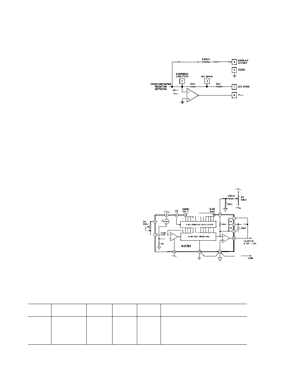
ANALOG CIRCUIT CONNECTIONS
Internal scaling resistors provided in the AD767 may be connected
to produce bipolar output voltage ranges of
±10, ±5 or ±2.5 V
or unipolar output voltage ranges of 0 to +5 V or 0 to +10 V.
Gain and offset drift are minimized in the AD767 because of the
thermal tracking of the scaling resistors with other device
components. Connections for various output voltage ranges are
shown in Table I.
Figure 1. Output Amplifier Voltage Range Scaling Circuit
UNIPOLAR CONFIGURATION (Figure 2)
This configuration will provide a unipolar 0 to +10 volt output
range. In this mode, the bipolar offset terminal, Pin 4, should be
grounded if not used for trimming.
STEP I … ZERO ADJUST
Turn all bits OFF and adjust zero trimmer R1, until the output
reads 0.000 volts (1 LSB = 2.44 mV). In most cases this trim is
not needed, and Pin 4 should be connected to Pin 5.
STEP II … GAIN ADJUST
Turn all bits ON and adjust 100
gain trimmer R2 until the
output is 9.9976 volts. (Full scale is adjusted to 1 LSB less than
nominal full scale of 10.000 volts.)
Figure 2. 0 to +10 V Unipolar Voltage Output
Table I. Output Voltage Range Connections
Output
Digital
Connect
Range
Input Codes
Pin 9 to
Pin 1 to
Pin 2 to
Pin 4 to
±10 V
Offset Binary
1
9
NC
6 (through 50
fixed or 100 trim resistor)
±5 V
Offset Binary
1 and 2
2 and 9
1 and 9
6 (through 50
fixed or 100 trim resistor)
±2.5 V
Offset Binary
2
3
9
6 (through 50
fixed or 100 trim resistor)
0 to +10 V
Straight Binary
1 and 2
2 and 9
1 and 9
5 (or optional trim – See Figure 2)
0 to +5 V
Straight Binary
2
3
9
5 (or optional trim – See Figure 2)
相关PDF资料 |
PDF描述 |
|---|---|
| AD5392BCPZ-5 | IC DAC 14BIT 8CHAN 5V 64LFCSP |
| AD5570BRSZ-REEL7 | IC DAC 16BIT SERIAL IN 16SSOP |
| AD5570BRSZ-REEL | IC DAC 16BIT SERIAL IN 16SSOP |
| AD7538AQ | IC DAC 14BIT W/BUFF 24-CDIP |
| VE-B52-MU | CONVERTER MOD DC/DC 15V 200W |
相关代理商/技术参数 |
参数描述 |
|---|---|
| AD767KPZ-REEL | 功能描述:IC DAC 12BIT W/AMP 28-PLCC RoHS:是 类别:集成电路 (IC) >> 数据采集 - 数模转换器 系列:- 产品培训模块:Data Converter Fundamentals DAC Architectures 标准包装:750 系列:- 设置时间:7µs 位数:16 数据接口:并联 转换器数目:1 电压电源:双 ± 功率耗散(最大):100mW 工作温度:0°C ~ 70°C 安装类型:表面贴装 封装/外壳:28-LCC(J 形引线) 供应商设备封装:28-PLCC(11.51x11.51) 包装:带卷 (TR) 输出数目和类型:1 电压,单极;1 电压,双极 采样率(每秒):143k |
| AD767SD/883B | 功能描述:数模转换器- DAC IC - 12-BIT D/A CONVERTER RoHS:否 制造商:Texas Instruments 转换器数量:1 DAC 输出端数量:1 转换速率:2 MSPs 分辨率:16 bit 接口类型:QSPI, SPI, Serial (3-Wire, Microwire) 稳定时间:1 us 最大工作温度:+ 85 C 安装风格:SMD/SMT 封装 / 箱体:SOIC-14 封装:Tube |
| AD767SD883B | 制造商:AD 制造商全称:Analog Devices 功能描述:Microprocessor-Compatible 12-Bit D/A Converter |
| AD768 | 制造商:AD 制造商全称:Analog Devices 功能描述:16-Bit, 30 MSPS D/A Converter |
| AD7680 | 制造商:AD 制造商全称:Analog Devices 功能描述:3mW, 100kSPS, 14-Bit ADC in 6-Lead SOT-23 |
发布紧急采购,3分钟左右您将得到回复。