- 您现在的位置:买卖IC网 > PDF目录1982 > AD7685CCPZRL (Analog Devices Inc)IC ADC 16BIT SAR 250KSPS 10LFCSP PDF资料下载
参数资料
| 型号: | AD7685CCPZRL |
| 厂商: | Analog Devices Inc |
| 文件页数: | 8/28页 |
| 文件大小: | 0K |
| 描述: | IC ADC 16BIT SAR 250KSPS 10LFCSP |
| 产品培训模块: | Motor Control |
| 设计资源: | Parametric Measurement Unit and Supporting Components for PAD Appls Using AD5522 and AD7685 (CN0104) Integrated Device Power Supply for PAD with Output Voltage Range 0 V to 25 V (CN0130) |
| 标准包装: | 5,000 |
| 系列: | PulSAR® |
| 位数: | 16 |
| 采样率(每秒): | 250k |
| 数据接口: | DSP,MICROWIRE?,QSPI?,串行,SPI? |
| 转换器数目: | 1 |
| 功率耗散(最大): | 15mW |
| 电压电源: | 模拟和数字 |
| 工作温度: | -40°C ~ 85°C |
| 安装类型: | 表面贴装 |
| 封装/外壳: | 10-WFDFN 裸露焊盘,CSP |
| 供应商设备封装: | 10-LFCSP-WD(3x3) |
| 包装: | 带卷 (TR) |
| 输入数目和类型: | 1 个伪差分,单极 |
| 配用: | EVAL-AD7685CBZ-ND - BOARD EVAL FOR AD7685 |
第1页第2页第3页第4页第5页第6页第7页当前第8页第9页第10页第11页第12页第13页第14页第15页第16页第17页第18页第19页第20页第21页第22页第23页第24页第25页第26页第27页第28页
AD7685
Rev. C | Page 16 of 28
DRIVER AMPLIFIER CHOICE
Although the AD7685 is easy to drive, the driver amplifier
needs to meet the following requirements:
The noise generated by the driver amplifier needs to be kept
as low as possible to preserve the SNR and transition noise
performance of the AD7685. Note that the AD7685 has a
noise much lower than most of the other 16-bit ADCs and,
therefore, can be driven by a noisier amplifier to meet a given
system noise specification. The noise coming from the
amplifier is filtered by the AD7685 analog input circuit low-
pass filter made by RIN and CIN or by an external filter, if one
is used. Because the typical noise of the AD7685 is 35 μV
rms, the SNR degradation due to the amplifier is
+
=
2
3dB
2
)
(
f
2
π
35
20log
N
LOSS
Ne
SNR
where:
f–3dB is the input bandwidth in MHz of the AD7685
(2 MHz) or the cutoff frequency of the input filter, if one is
used.
N is the noise gain of the amplifier (for example, 1 in buffer
configuration).
eN is the equivalent input noise voltage of the op amp, in
nV/√Hz.
For ac applications, the driver should have a THD
performance commensurate with the AD7685. Figure 17
shows the AD7685’s THD vs. frequency.
For multichannel, multiplexed applications, the driver
amplifier and the AD7685 analog input circuit must settle a
full-scale step onto the capacitor array at a 16-bit level
(0.0015%). In the amplifier’s data sheet, settling at 0.1% to
0.01% is more commonly specified. This could differ
significantly from the settling time at a 16-bit level and
should be verified prior to driver selection.
Table 9. Recommended Driver Amplifiers
Amplifier
Typical Application
Very low noise and low power
5 V single-supply, low power
5 V single-supply, low power
Low power, low noise, and low frequency
Very low noise and high frequency
Very low noise and high frequency
Small, low power and low frequency
High frequency and low power
VOLTAGE REFERENCE INPUT
The AD7685 voltage reference input, REF, has a dynamic input
impedance and should therefore be driven by a low impedance
source with efficient decoupling between the REF and GND
pins, as explained in the Layout section.
When REF is driven by a very low impedance source, for
10 μF (X5R, 0805 size) ceramic chip capacitor is appropriate for
optimum performance.
If an unbuffered reference voltage is used, the decoupling value
depends on the reference used. For instance, a 22 μF (X5R,
1206 size) ceramic chip capacitor is appropriate for optimum
performance using a low temperature drift ADR43x reference.
If desired, smaller reference decoupling capacitor values down
to 2.2 μF can be used with a minimal impact on performance,
especially DNL.
POWER SUPPLY
The AD7685 is specified over a wide operating range from
2.3 V to 5.5 V. It has, unlike other low voltage converters, a
noise low enough to design a 16-bit resolution system with low
supply and respectable performance. It uses two power supply
pins: a core supply VDD and a digital input/output interface
supply VIO. VIO allows direct interface with any logic between
1.8 V and VDD. To reduce the number of supplies needed, the
VIO and VDD can be tied together. The AD7685 is independent of
power supply sequencing between VIO and VDD. Additionally,
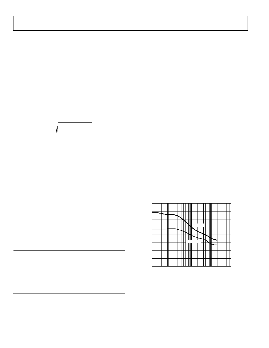
it is very insensitive to power supply variations over a wide
frequency range, as shown in Figure 31, which represents PSRR
over frequency.
02
96
8-
0
29
FREQUENCY (kHz)
10000
1
10
100
1000
P
S
RR
(
d
B)
110
80
90
100
70
60
50
40
30
VDD = 5V
VDD = 2.5V
Figure 31. PSRR vs. Frequency
相关PDF资料 |
PDF描述 |
|---|---|
| AD7686CCPZRL7 | IC ADC 16BIT SAR 500KSPS 10LFCSP |
| AD7687BCPZRL | IC ADC 16BIT SAR 250KSPS 10LFCSP |
| AD7688BCPZRL7 | IC ADC 16BIT SAR 500KSPS 10LFCSP |
| AD7689BCPZRL7 | IC ADC 16BIT 250KSPS 8CH 20LFCSP |
| AD7690BCPZRL | IC ADC 18BIT 400KSPS 10-LFCSP |
相关代理商/技术参数 |
参数描述 |
|---|---|
| AD7685CCPZRL7 | 功能描述:IC ADC 16BIT SAR 250KSPS 10LFCSP RoHS:是 类别:集成电路 (IC) >> 数据采集 - 模数转换器 系列:PulSAR® 其它有关文件:TSA1204 View All Specifications 标准包装:1 系列:- 位数:12 采样率(每秒):20M 数据接口:并联 转换器数目:2 功率耗散(最大):155mW 电压电源:模拟和数字 工作温度:-40°C ~ 85°C 安装类型:表面贴装 封装/外壳:48-TQFP 供应商设备封装:48-TQFP(7x7) 包装:Digi-Reel® 输入数目和类型:4 个单端,单极;2 个差分,单极 产品目录页面:1156 (CN2011-ZH PDF) 其它名称:497-5435-6 |
| AD7685CRM | 制造商:Analog Devices 功能描述:ADC Single SAR 250ksps 16-bit Serial 10-Pin MSOP |
| AD7685CRMRL7 | 制造商:Analog Devices 功能描述:ADC Single SAR 250ksps 16-bit Serial 10-Pin MSOP T/R |
| AD7685CRMZ | 功能描述:IC ADC 16BIT PSEUDO-DIFF 10-MSOP RoHS:是 类别:集成电路 (IC) >> 数据采集 - 模数转换器 系列:PulSAR® 标准包装:1 系列:microPOWER™ 位数:8 采样率(每秒):1M 数据接口:串行,SPI? 转换器数目:1 功率耗散(最大):- 电压电源:模拟和数字 工作温度:-40°C ~ 125°C 安装类型:表面贴装 封装/外壳:24-VFQFN 裸露焊盘 供应商设备封装:24-VQFN 裸露焊盘(4x4) 包装:Digi-Reel® 输入数目和类型:8 个单端,单极 产品目录页面:892 (CN2011-ZH PDF) 其它名称:296-25851-6 |
| AD7685CRMZRL7 | 功能描述:IC ADC 16BIT PSEUDO-DIFF 10MSOP RoHS:是 类别:集成电路 (IC) >> 数据采集 - 模数转换器 系列:PulSAR® 标准包装:1,000 系列:- 位数:12 采样率(每秒):300k 数据接口:并联 转换器数目:1 功率耗散(最大):75mW 电压电源:单电源 工作温度:0°C ~ 70°C 安装类型:表面贴装 封装/外壳:24-SOIC(0.295",7.50mm 宽) 供应商设备封装:24-SOIC 包装:带卷 (TR) 输入数目和类型:1 个单端,单极;1 个单端,双极 |
发布紧急采购,3分钟左右您将得到回复。