- 您现在的位置:买卖IC网 > PDF目录10106 > AD7703ARZ (Analog Devices Inc)IC ADC 20BIT LC2MOS 20-SOIC PDF资料下载
参数资料
| 型号: | AD7703ARZ |
| 厂商: | Analog Devices Inc |
| 文件页数: | 4/16页 |
| 文件大小: | 0K |
| 描述: | IC ADC 20BIT LC2MOS 20-SOIC |
| 标准包装: | 1 |
| 位数: | 20 |
| 采样率(每秒): | 4k |
| 数据接口: | 串行 |
| 转换器数目: | 1 |
| 功率耗散(最大): | 37mW |
| 电压电源: | 模拟和数字,双 ± |
| 工作温度: | -40°C ~ 85°C |
| 安装类型: | 表面贴装 |
| 封装/外壳: | 20-SOIC(0.295",7.50mm 宽) |
| 供应商设备封装: | 20-SOIC W |
| 包装: | 管件 |
| 输入数目和类型: | 1 个单端,单极;1 个单端,双极 |
REV. E
–12–
AD7703
INPUT SIGNAL CONDITIONING
Reference voltages from 1 V to 3 V may be used with the AD7703,
with little degradation in performance. Input ranges that cannot
be accommodated by this range of reference voltages may be
achieved by input signal conditioning. This may take the form of
gain to accommodate a smaller signal range, or passive attenua-
tion to reduce a larger input voltage range.
Source Resistance
If passive attenuators are used in front of the AD7703, care must
be taken to ensure that the source impedance is sufficiently low.
The dc input resistance for the AD7703 is over 1 G
W. In paral-
lel with this, there is a small dynamic load that varies with the
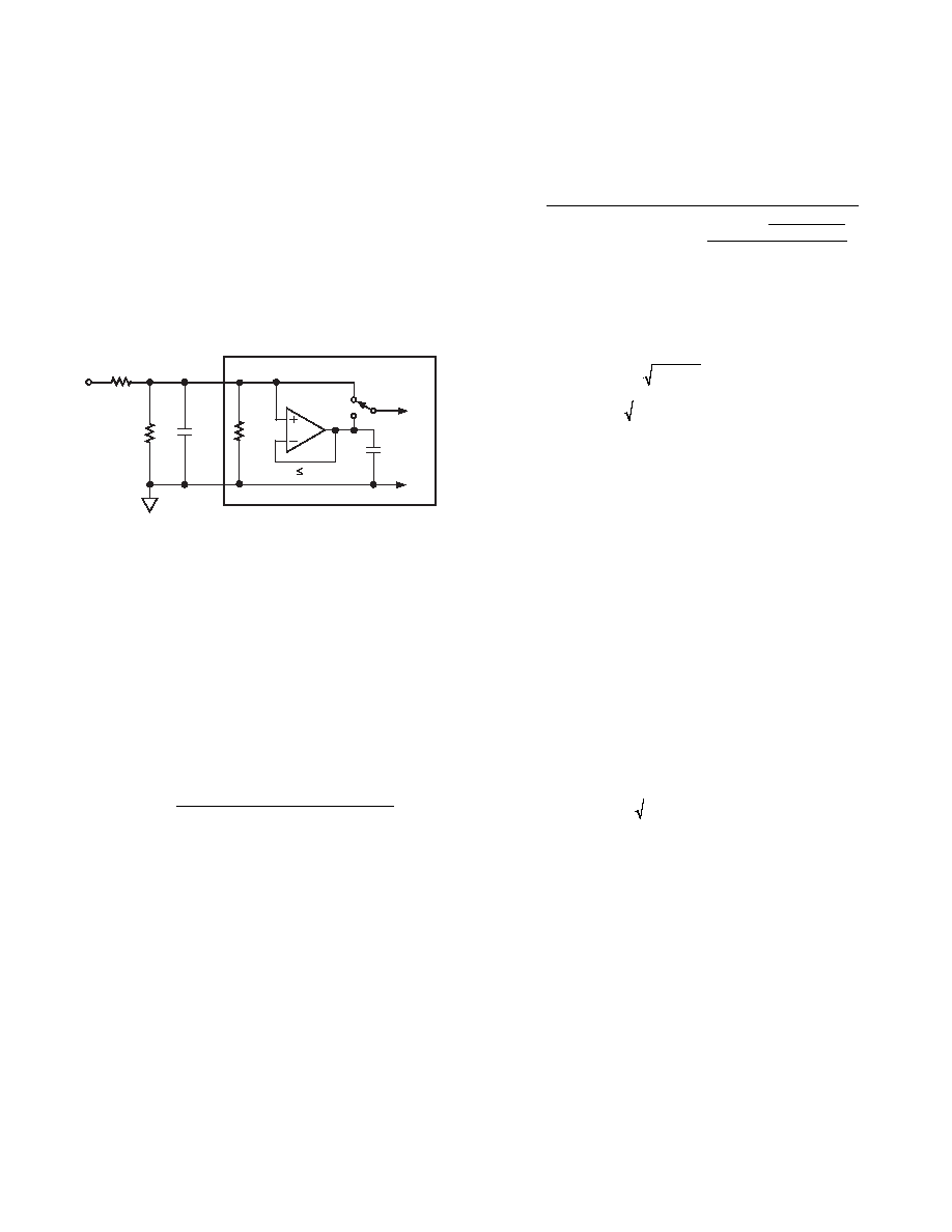
clock frequency (see Figure 14).
AIN
R1
R2
CEXT
AGND
AD7703
V OS 100mV
VIN
1G
CIN
10pF
Figure 14. Equivalent Input Circuit and Input Attenuator
Each time the analog input is sampled, a 10 pF capacitor draws a
charge packet of maximum 1 pC (10 pF
100 mV) from the
analog source with a frequency fCLKIN/256. For a 4.096 MHz
CLKIN, this yields an average current draw of 16 nA. After
each sample, the AD7703 allows 62 clock periods for the input
voltage to settle. The equation that defines settling time is
VO
=VIN [1– e–t/RC]
where VO, is the final settled value, VIN, is the value of the input
signal, R is the value of the input source resistance, and C is the
10 pF sample capacitor. The value of t is equal to 62/fCLKIN.
The following equation can be developed, which gives the maxi-
mum allowable source resistance, RS(MAX), for an error of VE:
R
fpF
mV V
S MAX
CLKIN
E
()
(
/
)
=
62
10
100
ln
Provided the source resistance is less than this value, the analog
input will settle within the desired error band in the requisite 62
clock periods. Insufficient settling leads to offset errors. These
can be calibrated in system calibration schemes.
If a limit of 600 nV (0.25 LSB at 20 bits) is set for the maximum
offset voltage, then the maximum allowable source resistance is
125 k
W from the above equation, assuming that there is no
external stray capacitance.
An RC filter may be added in front of the AD7703 to reduce
high frequency noise. With an external capacitor added from
AIN to AGND, the following equation will specify the maximum
allowable source resistance:
R
fC
C
mV
C
CC
V
S MAX
CLKIN
IN
EXT
IN
EXT
E
()
=
+
+
˙
62
100
ln
The practical limit to the maximum value of source resistance is
thermal (Johnson) noise. A practical resistor may be modeled as
an ideal (noiseless) resistor in series with a noise voltage source
or in parallel with a noise current source:
V
kTRf Volts
n
= 4
ikTf R Amperes
n
= 4/
where k is Boltzmann’s constant (1.38
10–23 J/K), and T is
temperature in degrees Kelvin (°C + 273).
Active signal conditioning circuits such as op amps generally do
not suffer from problems of high source impedance. Their open-
loop output resistance is normally only tens of ohms and, in any
case, most modern general-purpose op amps have sufficiently fast
closed-loop settling time for this not to be a problem. Offset volt-
age in op amps can be eliminated in a system calibration routine.
Antialias Considerations
The digital filter of the AD7703 does not provide any rejection
at integer multiples of the sampling frequency (nfCLKIN/256,
where n = 1, 2, 3 . . . ).
With a 4.096 MHz master clock, there are narrow (±10 Hz)
bands at 16 kHz, 32 kHz, 48 kHz, and so on, where noise passes
unattenuated to the output.
However, due to the AD7703’s high oversampling ratio of 800
(16 kHz to 20 Hz), these bands occupy only a small fraction of
the spectrum, and most broadband noise is filtered.
The reduction in broadband noise is given by
ee
f
e
out
in
C
S
in
==
20 035
/.
where ein and eout are rms noise terms referred to the input, fC is
the filter –3 dB corner frequency (fCLKIN/409600), and fS is the
sampling frequency (fCLKIN/256).
Since the ratio of fS to fCLKIN is fixed, the digital filter reduces
broadband white noise by 96.5% independent of the master
clock frequency.
相关PDF资料 |
PDF描述 |
|---|---|
| VI-BNP-MW-F3 | CONVERTER MOD DC/DC 13.8V 100W |
| AD9231BCPZRL7-80 | IC ADC 12BIT 80MSPS 64LFCSP |
| VI-231-IW-F1 | CONVERTER MOD DC/DC 12V 100W |
| VI-BNP-MW-F2 | CONVERTER MOD DC/DC 13.8V 100W |
| MS3102E24-11P | CONN RCPT 9POS BOX MNT W/PINS |
相关代理商/技术参数 |
参数描述 |
|---|---|
| AD7703BN | 功能描述:IC ADC 20BIT LC2MOS 20-DIP RoHS:否 类别:集成电路 (IC) >> 数据采集 - 模数转换器 系列:- 产品培训模块:Lead (SnPb) Finish for COTS Obsolescence Mitigation Program 标准包装:2,500 系列:- 位数:12 采样率(每秒):3M 数据接口:- 转换器数目:- 功率耗散(最大):- 电压电源:- 工作温度:- 安装类型:表面贴装 封装/外壳:SOT-23-6 供应商设备封装:SOT-23-6 包装:带卷 (TR) 输入数目和类型:- |
| AD7703BNZ | 功能描述:IC ADC 20BIT LC2MOS MONO 20DIP RoHS:是 类别:集成电路 (IC) >> 数据采集 - 模数转换器 系列:- 其它有关文件:TSA1204 View All Specifications 标准包装:1 系列:- 位数:12 采样率(每秒):20M 数据接口:并联 转换器数目:2 功率耗散(最大):155mW 电压电源:模拟和数字 工作温度:-40°C ~ 85°C 安装类型:表面贴装 封装/外壳:48-TQFP 供应商设备封装:48-TQFP(7x7) 包装:Digi-Reel® 输入数目和类型:4 个单端,单极;2 个差分,单极 产品目录页面:1156 (CN2011-ZH PDF) 其它名称:497-5435-6 |
| AD7703BQ | 制造商:AD 制造商全称:Analog Devices 功能描述:LC2MOS 20-Bit A/D Converter |
| AD7703BR | 功能描述:IC ADC 20BIT LC2MOS 20-SOIC RoHS:否 类别:集成电路 (IC) >> 数据采集 - 模数转换器 系列:- 产品培训模块:Lead (SnPb) Finish for COTS Obsolescence Mitigation Program 标准包装:2,500 系列:- 位数:12 采样率(每秒):3M 数据接口:- 转换器数目:- 功率耗散(最大):- 电压电源:- 工作温度:- 安装类型:表面贴装 封装/外壳:SOT-23-6 供应商设备封装:SOT-23-6 包装:带卷 (TR) 输入数目和类型:- |
| AD7703BR-REEL | 功能描述:IC ADC 20BIT LC2MOS MONO 20-SOIC RoHS:否 类别:集成电路 (IC) >> 数据采集 - 模数转换器 系列:- 标准包装:1 系列:- 位数:14 采样率(每秒):83k 数据接口:串行,并联 转换器数目:1 功率耗散(最大):95mW 电压电源:双 ± 工作温度:0°C ~ 70°C 安装类型:通孔 封装/外壳:28-DIP(0.600",15.24mm) 供应商设备封装:28-PDIP 包装:管件 输入数目和类型:1 个单端,双极 |
发布紧急采购,3分钟左右您将得到回复。