参数资料
| 型号: | AD7712AR |
| 厂商: | Analog Devices Inc |
| 文件页数: | 15/28页 |
| 文件大小: | 0K |
| 描述: | IC ADC SIGNAL COND LC2MOS 24SOIC |
| 标准包装: | 1 |
| 位数: | 24 |
| 采样率(每秒): | 1.03k |
| 数据接口: | 串行 |
| 转换器数目: | 1 |
| 功率耗散(最大): | 45mW |
| 电压电源: | 模拟和数字,双 ± |
| 工作温度: | -40°C ~ 85°C |
| 安装类型: | 表面贴装 |
| 封装/外壳: | 24-SOIC(0.295",7.50mm 宽) |
| 供应商设备封装: | 24-SOIC W |
| 包装: | 管件 |
| 输入数目和类型: | 1 个单端,单极;1 个差分,单极;1 个差分,双极 |
第1页第2页第3页第4页第5页第6页第7页第8页第9页第10页第11页第12页第13页第14页当前第15页第16页第17页第18页第19页第20页第21页第22页第23页第24页第25页第26页第27页第28页
REV. F
–22–
AD7712
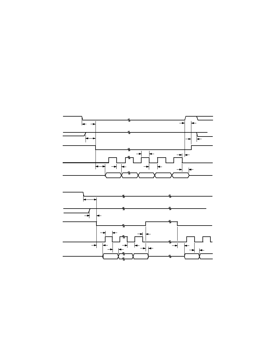
Figure 13a shows a read operation from the AD7712 where
RFS remains low for the duration of the data word transmis-
sion. With
DRDY low, the RFS input is brought low. The input
SCLK signal should be low between read and write operations.
RFS going low places the MSB of the word to be read on the
serial data line. All subsequent data bits are clocked out on a
high to low transition of the serial clock and are valid prior to
the following rising edge of this clock. The penultimate falling
edge of SCLK clocks out the LSB and the final falling edge
resets the
DRDY line high. This rising edge of DRDY turns off
the serial data output.
Figure 13b shows a timing diagram for a read operation where
RFS returns high during the transmission of the word and
returns low again to access the rest of the data-word. Timing
parameters and functions are very similar to that outlined for
Figure 13a, but Figure 13b has a number of additional times to
show timing relationships when
RFS returns high in the middle
of transferring a word.
RFS should return high during a low time of SCLK. On the
rising edge of
RFS, the SDATA output is turned off. DRDY
remains low and will remain low until all bits of the data-word
are read from the AD7712, regardless of the number of times
RFS changes state during the read operation. Depending on the
time between the falling edge of SCLK and the rising edge of
RFS, the next bit (BIT N + 1) may appear on the data bus
before
RFS goes high. When RFS returns low again, it activates
the SDATA output. When the entire word is transmitted, the
DRDY line will go high, turning off the SDATA output as per
Figure 13a.
RFS (I)
SCLK (I)
SDATA (O)
LSB
MSB
THREE-STATE
A0 (I)
DRDY (O)
t20
t21
t22
t23
t24
t25
t26
t27
t28
t29
Figure 13a. External Clocking Mode, Output Data Read Operation
THREE-STATE
MSB
BIT N
BIT N+1
SDATA (O)
SCLK (I)
RFS (I)
A0 (I)
DRDY (O)
t20
t22
t26
t24
t25
t27
t31
t24
t25
t30
Figure 13b. External Clocking Mode, Output Data Read Operation (
RFS Returns High during Read Operation)
相关PDF资料 |
PDF描述 |
|---|---|
| AD7713AN | IC ADC 24BIT SIGMA-DELTA 24-DIP |
| AD7714ARS-3 | IC ADC 24BIT SIGMA-DELTA 28SSOP |
| AD7715ANZ-3 | IC ADC 16BIT SIGMA-DELTA 16DIP |
| AD7716BSZ | IC ADC 22BIT SIGMA-DELTA 44-MQFP |
| AD7718BRU-REEL7 | IC ADC 24BIT R-R 8/10CH 28-TSSOP |
相关代理商/技术参数 |
参数描述 |
|---|---|
| AD7712AR-REEL | 制造商:Analog Devices 功能描述:ADC Single Delta-Sigma 1.028ksps 24-bit Serial 24-Pin SOIC W T/R 制造商:Analog Devices 功能描述:ADC SGL DELTA-SIGMA 1.028KSPS 24BIT SERL 24SOIC W - Tape and Reel |
| AD7712AR-REEL7 | 功能描述:IC ADC 24BIT SGNL CONDTNR 24SOIC RoHS:否 类别:集成电路 (IC) >> 数据采集 - 模数转换器 系列:- 标准包装:1 系列:- 位数:14 采样率(每秒):83k 数据接口:串行,并联 转换器数目:1 功率耗散(最大):95mW 电压电源:双 ± 工作温度:0°C ~ 70°C 安装类型:通孔 封装/外壳:28-DIP(0.600",15.24mm) 供应商设备封装:28-PDIP 包装:管件 输入数目和类型:1 个单端,双极 |
| AD7712ARZ | 功能描述:IC ADC SIGNAL COND LC2MOS 24SOIC RoHS:是 类别:集成电路 (IC) >> 数据采集 - 模数转换器 系列:- 标准包装:1 系列:microPOWER™ 位数:8 采样率(每秒):1M 数据接口:串行,SPI? 转换器数目:1 功率耗散(最大):- 电压电源:模拟和数字 工作温度:-40°C ~ 125°C 安装类型:表面贴装 封装/外壳:24-VFQFN 裸露焊盘 供应商设备封装:24-VQFN 裸露焊盘(4x4) 包装:Digi-Reel® 输入数目和类型:8 个单端,单极 产品目录页面:892 (CN2011-ZH PDF) 其它名称:296-25851-6 |
| AD7712ARZ | 制造商:Analog Devices 功能描述:A/D Converter (A-D) IC |
| AD7712ARZ-REEL | 功能描述:IC ADC 24BIT SGNL CONDTNR 24SOIC RoHS:是 类别:集成电路 (IC) >> 数据采集 - 模数转换器 系列:- 标准包装:1 系列:- 位数:14 采样率(每秒):83k 数据接口:串行,并联 转换器数目:1 功率耗散(最大):95mW 电压电源:双 ± 工作温度:0°C ~ 70°C 安装类型:通孔 封装/外壳:28-DIP(0.600",15.24mm) 供应商设备封装:28-PDIP 包装:管件 输入数目和类型:1 个单端,双极 |
发布紧急采购,3分钟左右您将得到回复。