- 您现在的位置:买卖IC网 > PDF目录10211 > AD7714AR-5REEL (Analog Devices Inc)IC ADC 24BIT SIGMA-DELTA 24-SOIC PDF资料下载
参数资料
| 型号: | AD7714AR-5REEL |
| 厂商: | Analog Devices Inc |
| 文件页数: | 23/40页 |
| 文件大小: | 0K |
| 描述: | IC ADC 24BIT SIGMA-DELTA 24-SOIC |
| 标准包装: | 1,000 |
| 位数: | 24 |
| 采样率(每秒): | 1k |
| 数据接口: | DSP,MICROWIRE?,QSPI?,串行,SPI? |
| 转换器数目: | 1 |
| 功率耗散(最大): | 7mW |
| 电压电源: | 模拟和数字 |
| 工作温度: | -40°C ~ 85°C |
| 安装类型: | 表面贴装 |
| 封装/外壳: | 24-SOIC(0.295",7.50mm 宽) |
| 供应商设备封装: | 24-SOIC W |
| 包装: | 带卷 (TR) |
| 输入数目和类型: | 3 个差分,单极;3 个差分,双极;5 个伪差分,单极;5 个伪差分,双极 |
| 配用: | EVAL-AD7714-3EBZ-ND - BOARD EVAL FOR AD7714 |
第1页第2页第3页第4页第5页第6页第7页第8页第9页第10页第11页第12页第13页第14页第15页第16页第17页第18页第19页第20页第21页第22页当前第23页第24页第25页第26页第27页第28页第29页第30页第31页第32页第33页第34页第35页第36页第37页第38页第39页第40页
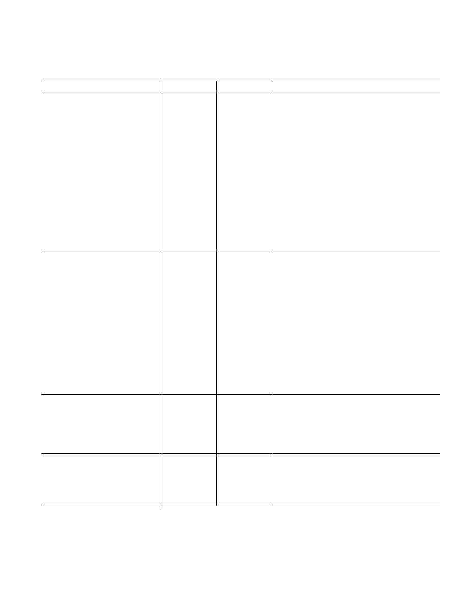
Parameter
A Versions
Units
Conditions/Comments
STATIC PERFORMANCE
No Missing Codes
24
Bits min
Guaranteed by Design. Bipolar Mode. For Filter Notches
≤ 60 Hz
22
Bits min
For Filter Notch = 100 Hz
18
Bits min
For Filter Notch = 250 Hz
15
Bits min
For Filter Notch = 500 Hz
12
Bits min
For Filter Notch = 1 kHz
Output Noise
See Tables I to IV
Depends on Filter Cutoffs and Selected Gain
Integral Nonlinearity
±0.0015
% of FSR max
Filter Notches
≤ 60 Hz
Unipolar Offset Error
See Note 2
Unipolar Offset Drift3
0.4
V/°C typ
For Gains of 1, 2, 4
0.1
V/°C typ
For Gains of 8, 16, 32, 64, 128
Bipolar Zero Error
See Note 2
Bipolar Zero Drift3
0.4
V/°C typ
For Gains of 1, 2, 4
0.1
V/°C typ
For Gains of 8, 16, 32, 64, 128
Positive Full-Scale Error4
See Note 2
Full-Scale Drift
3, 5
0.4
V/°C typ
For Gains of 1, 2, 4
0.1
V/°C typ
For Gains of 8, 16, 32, 64, 128
Gain Error6
See Note 2
Gain Drift3, 7
0.2
ppm of FSR/
°C typ
Bipolar Negative Full-Scale Error
±0.003
% of FSR max
Typically
±0.0004%
Bipolar Negative Full-Scale Drift
3
1
V/°C typ
For Gains of 1, 2, 4
0.6
V/°C typ
For Gains of 8, 16, 32, 64, 128
ANALOG INPUTS/REFERENCE INPUTS
Specifications for AIN and REF IN Unless Noted
Input Common-Mode Rejection (CMR)
90
dB min
At DC. Typically 102 dB.
Normal-Mode 50 Hz Rejection8
100
dB min
For Filter Notches of 10 Hz, 25 Hz, 50 Hz,
±0.02 × f
NOTCH
Normal-Mode 60 Hz Rejection
8
100
dB min
For Filter Notches of 10 Hz, 30 Hz, 60 Hz,
±0.02 × f
NOTCH
Common-Mode 50 Hz Rejection8
150
dB min
For Filter Notches of 10 Hz, 25 Hz, 50 Hz,
±0.02 × f
NOTCH
Common-Mode 60 Hz Rejection8
150
dB min
For Filter Notches of 10 Hz, 30 Hz, 60 Hz,
±0.02 × f
NOTCH
Common-Mode Voltage Range9
AGND to AVDD
V min to V max
AIN for BUFFER = 0 and REF IN
Absolute AIN/REF IN Voltage9
AGND – 30 mV
V min
AIN for BUFFER = 0 and REF IN
AVDD + 30 mV
V max
Absolute/Common-Mode AIN Voltage9
AGND + 50 mV
V min
BUFFER = 1
AVDD – 1.5 V
V max
AIN Input Current8
1
nA max
AIN Sampling Capacitance8
7
pF max
AIN Differential Voltage Range
10
0 to +VREF/GAIN
11
nom
Unipolar Input Range (B/U Bit of Filter High Register = 1)
±V
REF/GAIN
nom
Bipolar Input Range (B/U Bit of Filter High Register = 0)
AIN Input Sampling Rate, fS
GAIN
× f
CLK IN/64
For Gains of 1, 2, 4
fCLK IN/8
For Gains of 8, 16, 32, 64, 128
REF IN(+) – REF IN(–) Voltage
+1.25
V nom
±1% for Specified Performance. Part Functions with
Lower VREF
REF IN Input Sampling Rate, fS
fCLK IN/64
LOGIC INPUTS
Input Current
±10
A max
All Inputs Except MCLK IN
VINL, Input Low Voltage
0.4
V max
VINH, Input High Voltage
2.0
V min
MCLK IN Only
VINL, Input Low Voltage
0.4
V max
VINH, Input High Voltage
2.5
V min
LOGIC OUTPUTS (Including MCLK OUT)
VOL, Output Low Voltage
0.4
V max
ISINK = 100 A Except for MCLK OUT
12
VOH, Output High Voltage
DVDD – 0.6
V min
ISOURCE = 100 A Except for MCLK OUT
12
Floating State Leakage Current
±10
A max
Floating State Output Capacitance13
9
pF typ
Data Output Coding
Binary
Unipolar Mode
Offset Binary
Bipolar Mode
NOTES
7Gain Error Drift does not include Unipolar Offset Drift/Bipolar Zero Drift. It is effectively the drift of the part if zero-scale calibrations only were performed as is the case with
background calibration.
8These numbers are guaranteed by design and/or characterization.
9The common-mode voltage range on the input pairs applies provided the absolute input voltage specification is obeyed.
10The input voltage range on the analog inputs is given here with respect to the voltage on the respective negative input of its differential or pseudo-differential pair. See Table VII
for which inputs form differential pairs.
11V
REF = REF IN(+) – REF IN(–).
12These logic output levels apply to the MCLK OUT output only when it is loaded with a single CMOS load.
13Sample tested at +25
°C to ensure compliance.
14See Burnout Current section.
AD7714-3–SPECIFICATIONS (AV
DD = +3.3 V, DVDD = +3.3 V, REF IN(+) = +1.25 V; REF IN(–) = AGND;
fCLK IN = 2.4576 MHz unless otherwise noted. All specifications TMIN to TMAX unless otherwise noted.)
AD7714
REV. C
–3–
相关PDF资料 |
PDF描述 |
|---|---|
| SA572DR2G | IC COMPANDOR 2CHAN GAIN 16-SOIC |
| SP3085EEN-L/TR | IC TXRX RS485/RS422 ESD 8NSOIC |
| AD7776AR-REEL | IC ADC 10BIT 1CH HS 24-SOIC T/R |
| CS3106A-12S-60S | CONN PLUG 2POS STRAIGHT W/SCKT |
| AD7853LAR | IC ADC 12BIT SRL 200KSPS 24-SOIC |
相关代理商/技术参数 |
参数描述 |
|---|---|
| AD7714AR-5Z | 制造商:Analog Devices 功能描述:ADC 24BIT 5CH PGA 24SOIC 制造商:Analog Devices 功能描述:ADC, 24BIT, 5CH PGA, 24SOIC; Resolution (Bits):24bit; Sampling Rate:1kSPS; Supply Voltage Type:Single; Supply Voltage Min:4.75V; Supply Voltage Max:5.25V; Supply Current:1.1mA; Digital IC Case Style:SOIC; No. of Pins:24; Input ;RoHS Compliant: Yes |
| AD7714ARS-3 | 功能描述:IC ADC 24BIT SIGMA-DELTA 28SSOP RoHS:否 类别:集成电路 (IC) >> 数据采集 - 模数转换器 系列:- 标准包装:1,000 系列:- 位数:12 采样率(每秒):300k 数据接口:并联 转换器数目:1 功率耗散(最大):75mW 电压电源:单电源 工作温度:0°C ~ 70°C 安装类型:表面贴装 封装/外壳:24-SOIC(0.295",7.50mm 宽) 供应商设备封装:24-SOIC 包装:带卷 (TR) 输入数目和类型:1 个单端,单极;1 个单端,双极 |
| AD7714ARS-3REEL | 功能描述:IC ADC 24BIT SIGMA-DELTA 28SSOP RoHS:否 类别:集成电路 (IC) >> 数据采集 - 模数转换器 系列:- 标准包装:1,000 系列:- 位数:12 采样率(每秒):300k 数据接口:并联 转换器数目:1 功率耗散(最大):75mW 电压电源:单电源 工作温度:0°C ~ 70°C 安装类型:表面贴装 封装/外壳:24-SOIC(0.295",7.50mm 宽) 供应商设备封装:24-SOIC 包装:带卷 (TR) 输入数目和类型:1 个单端,单极;1 个单端,双极 |
| AD7714ARS-5 | 功能描述:IC ADC SIGNAL COND 5V 28-SSOP RoHS:否 类别:集成电路 (IC) >> 数据采集 - 模数转换器 系列:- 标准包装:1,000 系列:- 位数:12 采样率(每秒):300k 数据接口:并联 转换器数目:1 功率耗散(最大):75mW 电压电源:单电源 工作温度:0°C ~ 70°C 安装类型:表面贴装 封装/外壳:24-SOIC(0.295",7.50mm 宽) 供应商设备封装:24-SOIC 包装:带卷 (TR) 输入数目和类型:1 个单端,单极;1 个单端,双极 |
| AD7714ARS-5REEL | 功能描述:IC ADC 24BIT SIGMA-DELTA 28SSOP RoHS:否 类别:集成电路 (IC) >> 数据采集 - 模数转换器 系列:- 标准包装:1,000 系列:- 位数:12 采样率(每秒):300k 数据接口:并联 转换器数目:1 功率耗散(最大):75mW 电压电源:单电源 工作温度:0°C ~ 70°C 安装类型:表面贴装 封装/外壳:24-SOIC(0.295",7.50mm 宽) 供应商设备封装:24-SOIC 包装:带卷 (TR) 输入数目和类型:1 个单端,单极;1 个单端,双极 |
发布紧急采购,3分钟左右您将得到回复。