- 您现在的位置:买卖IC网 > PDF目录10667 > AD7732BRUZ (Analog Devices Inc)IC ADC 24BIT 2-CH 28-TSSOP PDF资料下载
参数资料
| 型号: | AD7732BRUZ |
| 厂商: | Analog Devices Inc |
| 文件页数: | 5/32页 |
| 文件大小: | 0K |
| 描述: | IC ADC 24BIT 2-CH 28-TSSOP |
| 标准包装: | 50 |
| 位数: | 24 |
| 采样率(每秒): | 15.4k |
| 数据接口: | DSP,MICROWIRE?,QSPI?,串行,SPI? |
| 转换器数目: | 1 |
| 功率耗散(最大): | 100mW |
| 电压电源: | 模拟和数字 |
| 工作温度: | -40°C ~ 105°C |
| 安装类型: | 表面贴装 |
| 封装/外壳: | 28-TSSOP(0.173",4.40mm 宽) |
| 供应商设备封装: | 28-TSSOP |
| 包装: | 管件 |
| 输入数目和类型: | 2 个差分,单极;2 个差分,双极 |
| 产品目录页面: | 779 (CN2011-ZH PDF) |
| 配用: | EVAL-AD7732EBZ-ND - BOARD EVAL FOR AD7732 |
第1页第2页第3页第4页当前第5页第6页第7页第8页第9页第10页第11页第12页第13页第14页第15页第16页第17页第18页第19页第20页第21页第22页第23页第24页第25页第26页第27页第28页第29页第30页第31页第32页
AD7732
Rev. A | Page 13 of 32
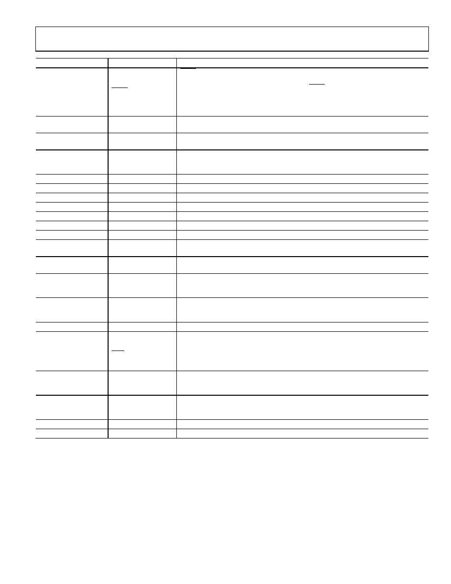
Pin No.
Mnemonic
Description
8
SYNC/P1
SYNC/Digital Input/Digital Output. The pin direction is determined by the P1 DIR bit;
the digital value can be read/written as the P1 bit in the I/O port register. When the
SYNC bit in the I/O port register is set to 1, the SYNC/P1 pin can be used to synchronize
the AD7732 modulator and digital filter with other devices in the system. The digital
voltage is referenced to analog supplies. When configured as an input, the pin should be
tied high or low.
9
RA
RA, in association with RB and BIAS0(+), can be used to level shift the positive analog
input 0. In normal circuit configuration, this pin is left open circuit.
10
RB
RB, in association with RA and BIAS0(+), can be used to level shift the positive analog
input 0. In normal circuit configuration, this pin is left open circuit.
11
BIAS1(+)
This input is used to level shift the positive analog input 1. This signal is used to ensure
that the differential signal seen by the internal buffer amplifier is within its common-
mode range. BIAS pins will normally be connected to 2.5 V.
12
AIN1(+)
Positive Analog Input Channel 1.
13
AIN0(+)
Positive Analog Input Channel 0.
14
BIAS0(+)
Voltage Bias for Positive Analog Input 0. This pin has the same function as BIAS1(+).
15
BIAS0(–)
Voltage Bias for Negative Analog Input 0. This pin has the same function as BIAS1(+).
16
AIN0(–)
Negative Analog Input Channel 0.
17
AIN1(–)
Negative Analog Input Channel 1.
18
BIAS1(–)
Voltage Bias for Negative Analog Input 1. This pin has the same function as BIAS1(+).
19
RC
RC, in association with RD and BIAS0(–), can be used to level shift the negative analog
input 0. In normal circuit configuration, this pin is left open circuit.
20
RD
RD, in association with RC and BIAS0(–), can be used to level shift the negative analog
input 0. In normal circuit configuration, this pin is left open circuit.
21
REFIN(+)
Positive Terminal of the Differential Reference Input. REFIN(+) voltage potential can lie
anywhere between AVDD and AGND. In normal circuit configuration, this pin should be
connected to a 2.5 V reference voltage.
22
REFIN(–)
Negative Terminal of the Differential Reference Input. REFIN(–) voltage potential can lie
anywhere between AVDD and AGND. In normal circuit configuration, this pin should be
connected to a 0 V reference voltage.
23
AGND
Ground Reference Point for Analog Circuitry.
24
RDY
Logic Output. Used as a status output in both conversion mode and calibration mode. In
conversion mode, a falling edge on this output indicates that either any channel or all
channels have unread data available, according to the RDYFN bit in the I/O port register.
In calibration mode, a falling edge on this output indicates that calibration is complete
(see the Digital Interface Description section for more details).
25
DOUT
Serial data output with serial data being read from the output shift register on the part.
This output shift register can contain information from any AD7732 register, depending
on the address bits of the communications register.
26
DIN
Serial data input (Schmitt triggered) with serial data being written to the input shift
register on the part. Data from this input shift register is transferred to any AD7732
register, depending on the address bits of the communications register.
27
DVDD
Digital Supply Voltage, 3 V or 5 V Nominal.
28
DGND
Ground Reference Point for Digital Circuitry.
相关PDF资料 |
PDF描述 |
|---|---|
| LTC1418CG#PBF | IC A/D CONV 14BIT SRL&PAR 28SSOP |
| AD7574JNZ | IC ADC 8BIT CMOS 5V 18-DIP |
| AD7767BRUZ | ADC 24BIT 128KSPS SAR 16-TSSOP |
| AD7660ASTZ | IC ADC 16BIT UNIPOLAR 48-LQFP |
| VE-J11-MW-F1 | CONVERTER MOD DC/DC 12V 100W |
相关代理商/技术参数 |
参数描述 |
|---|---|
| AD7732BRUZ | 制造商:Analog Devices 功能描述:IC 24BIT ADC SMD 7732 TSSOP28 |
| AD7732BRUZ-REEL | 功能描述:IC ADC 24BIT 2CH SIG-DEL 28TSSOP RoHS:是 类别:集成电路 (IC) >> 数据采集 - 模数转换器 系列:- 标准包装:1,000 系列:- 位数:12 采样率(每秒):300k 数据接口:并联 转换器数目:1 功率耗散(最大):75mW 电压电源:单电源 工作温度:0°C ~ 70°C 安装类型:表面贴装 封装/外壳:24-SOIC(0.295",7.50mm 宽) 供应商设备封装:24-SOIC 包装:带卷 (TR) 输入数目和类型:1 个单端,单极;1 个单端,双极 |
| AD7732BRUZ-REEL7 | 功能描述:IC ADC 24BIT 2CH SIG-DEL 28TSSOP RoHS:是 类别:集成电路 (IC) >> 数据采集 - 模数转换器 系列:- 标准包装:1,000 系列:- 位数:12 采样率(每秒):300k 数据接口:并联 转换器数目:1 功率耗散(最大):75mW 电压电源:单电源 工作温度:0°C ~ 70°C 安装类型:表面贴装 封装/外壳:24-SOIC(0.295",7.50mm 宽) 供应商设备封装:24-SOIC 包装:带卷 (TR) 输入数目和类型:1 个单端,单极;1 个单端,双极 |
| AD7734 | 制造商:AD 制造商全称:Analog Devices 功能描述:4-Channel, +-10 V Input Range, High Throughput, 24-Bit sigma ∆ ADC |
| AD7734BRU | 功能描述:IC ADC 24BIT 4-CH 28-TSSOP RoHS:否 类别:集成电路 (IC) >> 数据采集 - 模数转换器 系列:- 标准包装:1,000 系列:- 位数:12 采样率(每秒):300k 数据接口:并联 转换器数目:1 功率耗散(最大):75mW 电压电源:单电源 工作温度:0°C ~ 70°C 安装类型:表面贴装 封装/外壳:24-SOIC(0.295",7.50mm 宽) 供应商设备封装:24-SOIC 包装:带卷 (TR) 输入数目和类型:1 个单端,单极;1 个单端,双极 |
发布紧急采购,3分钟左右您将得到回复。