- 您现在的位置:买卖IC网 > PDF目录22159 > AD7740KRM (Analog Devices Inc)IC CONVERTER V TO FREQ 8-MSOP PDF资料下载
参数资料
| 型号: | AD7740KRM |
| 厂商: | Analog Devices Inc |
| 文件页数: | 4/11页 |
| 文件大小: | 144K |
| 描述: | IC CONVERTER V TO FREQ 8-MSOP |
| 标准包装: | 50 |
| 类型: | 电压至频率 |
| 频率 - 最大: | 1MHz |
| 全量程: | ±50ppm/°C |
| 线性: | ±0.012% |
| 安装类型: | 表面贴装 |
| 封装/外壳: | 8-TSSOP,8-MSOP(0.118",3.00mm 宽) |
| 供应商设备封装: | 8-MSOP |
| 包装: | 管件 |
4
PIN FUNCTION DESCRIPTIONS
8-LEAD microSOIC PIN NUMBERS*
Pin
No. Mnemonic Function
1 CLKOUT The crystal/resonator is tied between this pin and CLKIN. In the case of an external clock driving CLKIN, an
inverted clock signal appears on this pin and can be used to drive other circuitry provided it is buffered rst.
2 CLKIN The master clock for the device may be in the form of a crystal/resonator tied between this pin and CLKOUT.
An external CMOS-compatible clock may also be applied to this input as the clock for the device. If CLKIN
is inactive low for 1 ms (typ), the AD7740 automatically enters power-down.
3 GND
Ground reference for all the circuitry on-chip.
4 REFIN/OUT Voltage Reference Input. This is the reference input to the core of the VFC and denes the span of the VFC.
If this pin is left unconnected, the internal 2.5 V reference is the default reference. Alternatively, a precision
external reference may be used to overdrive the internal reference. The internal reference has high output
impedance in order to allow it to be overdriven.
5 VIN
The analog input to the VFC. It has a nominal input range from 0 V to V
REF
which corresponds to an output
frequency of 10% f
CLKIN
to 90% f
CLKIN
. It has a ?50 mV overrange. If buffered, it draws virtually no current
from whatever source is driving it.
6 VDD
Power Supply Input. These parts can be operated at 3.3 V ?10% or 5 V ?5%. The supply should be
adequately decoupled with a 10 礔 and a 0.1 礔 capacitor to GND.
7 FOUT Frequency Output. FOUT goes from 10% to 90% of f
CLKIN
, depending on VIN.
8 BUF
Buffered Mode Select Pin. When BUF is tied low, the VIN input is unbuffered and the range on the VIN
pin is 0.15 V to VDD + 0.15 V. When it is tied high, VIN is buffered and the range on the VIN pin
is restricted to 0.1 V to VDD 0.2 V.
*Note that the SOT-23 and microSOIC packages have different pinouts.
ORDERING GUIDE
Package
Branding
Model
Temperature Range
Package Description
Option
Information
AD7740KRM
0癈 to 85癈
microSOIC Package
RM-8
VOK
AD7740YRT
40癈 to +105癈
SOT-23 Package
RT-8
VOY
AD7740YRM
40癈 to +105癈
microSOIC Package
RM-8
VOY
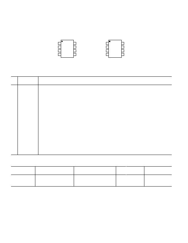
PIN CONFIGURATIONS
8-Lead microSOIC
microSOIC
TOP VIEW
(Not to Scale)
8
7
6
5
1
2
3
4
CLKOUT
CLKIN
GND
REFIN/OUT
BUF
FOUT
VDD
VIN
AD7740
8-Lead SOT-23
SOT-23
TOP VIEW
(Not to Scale)
8
7
6
5
1
2
3
4
BUF
OUT
VDD
VIN
CLKOUT
CLKIN
GND
REFIN/OUT
AD7740
REV. A
AD7740
相关PDF资料 |
PDF描述 |
|---|---|
| R0.25D12-1205/H | CONV DC/DC 0.25W 12VIN +/-5V OUT |
| R0.25D12-053.3/P | CONV DC/DC 0.25W 5VIN +/-3.3VOUT |
| R0.25D12-0509/P | CONV DC/DC 0.25W 5VIN +/-9VOUT |
| AD7740YRM-REEL7 | IC CONVERTER V TO FREQ 8-MSOP |
| VJ1210Y224KBBAT4X | CAP CER 0.22UF 100V 10% X7R 1210 |
相关代理商/技术参数 |
参数描述 |
|---|---|
| AD7740KRM-REEL | 制造商:Analog Devices 功能描述:VFC Sync 1MHz 8-Pin MSOP T/R 制造商:Analog Devices 功能描述:VFC SYNC 1MHZ 8MSOP - Tape and Reel |
| AD7740KRM-REEL7 | 功能描述:IC CONVERTER V TO FREQ 8-MSOP RoHS:否 类别:集成电路 (IC) >> PMIC - V/F 和 F/V 转换器 系列:- 标准包装:1 系列:- 类型:频率至电压 频率 - 最大:10kHz 全量程:- 线性:±0.3% 安装类型:表面贴装 封装/外壳:8-SOIC(0.154",3.90mm 宽) 供应商设备封装:8-SOIC 包装:Digi-Reel® 其它名称:LM2917MX-8/NOPBDKR |
| AD7740KRMZ | 功能描述:IC CONV SYNC VOLT-FREQ 8-MSOP RoHS:是 类别:集成电路 (IC) >> PMIC - V/F 和 F/V 转换器 系列:- 标准包装:1 系列:- 类型:频率至电压 频率 - 最大:10kHz 全量程:- 线性:±0.3% 安装类型:表面贴装 封装/外壳:8-SOIC(0.154",3.90mm 宽) 供应商设备封装:8-SOIC 包装:Digi-Reel® 其它名称:LM2917MX-8/NOPBDKR |
| AD7740KRMZ | 制造商:Analog Devices 功能描述:Voltage / Frequency (V/F & F/V) Converte |
| AD7740KRMZ-REEL | 功能描述:IC CONVERTER VOLT TO FREQ 8MSOP RoHS:是 类别:集成电路 (IC) >> PMIC - V/F 和 F/V 转换器 系列:- 标准包装:1 系列:- 类型:频率至电压 频率 - 最大:10kHz 全量程:- 线性:±0.3% 安装类型:表面贴装 封装/外壳:8-SOIC(0.154",3.90mm 宽) 供应商设备封装:8-SOIC 包装:Digi-Reel® 其它名称:LM2917MX-8/NOPBDKR |
发布紧急采购,3分钟左右您将得到回复。