- 您现在的位置:买卖IC网 > PDF目录10143 > AD7778ASZ (Analog Devices Inc)IC ADC 10BIT 8CHAN HS 44-MQFP PDF资料下载
参数资料
| 型号: | AD7778ASZ |
| 厂商: | Analog Devices Inc |
| 文件页数: | 10/12页 |
| 文件大小: | 0K |
| 描述: | IC ADC 10BIT 8CHAN HS 44-MQFP |
| 标准包装: | 1 |
| 位数: | 10 |
| 采样率(每秒): | 378k |
| 数据接口: | 并联 |
| 转换器数目: | 1 |
| 电压电源: | 单电源 |
| 工作温度: | -40°C ~ 85°C |
| 安装类型: | 表面贴装 |
| 封装/外壳: | 44-QFP |
| 供应商设备封装: | 44-MQFP(10x10) |
| 包装: | 托盘 |
| 输入数目和类型: | 8 个单端,单极 |
AD7776/AD7777/AD7778
–7–
REV. A
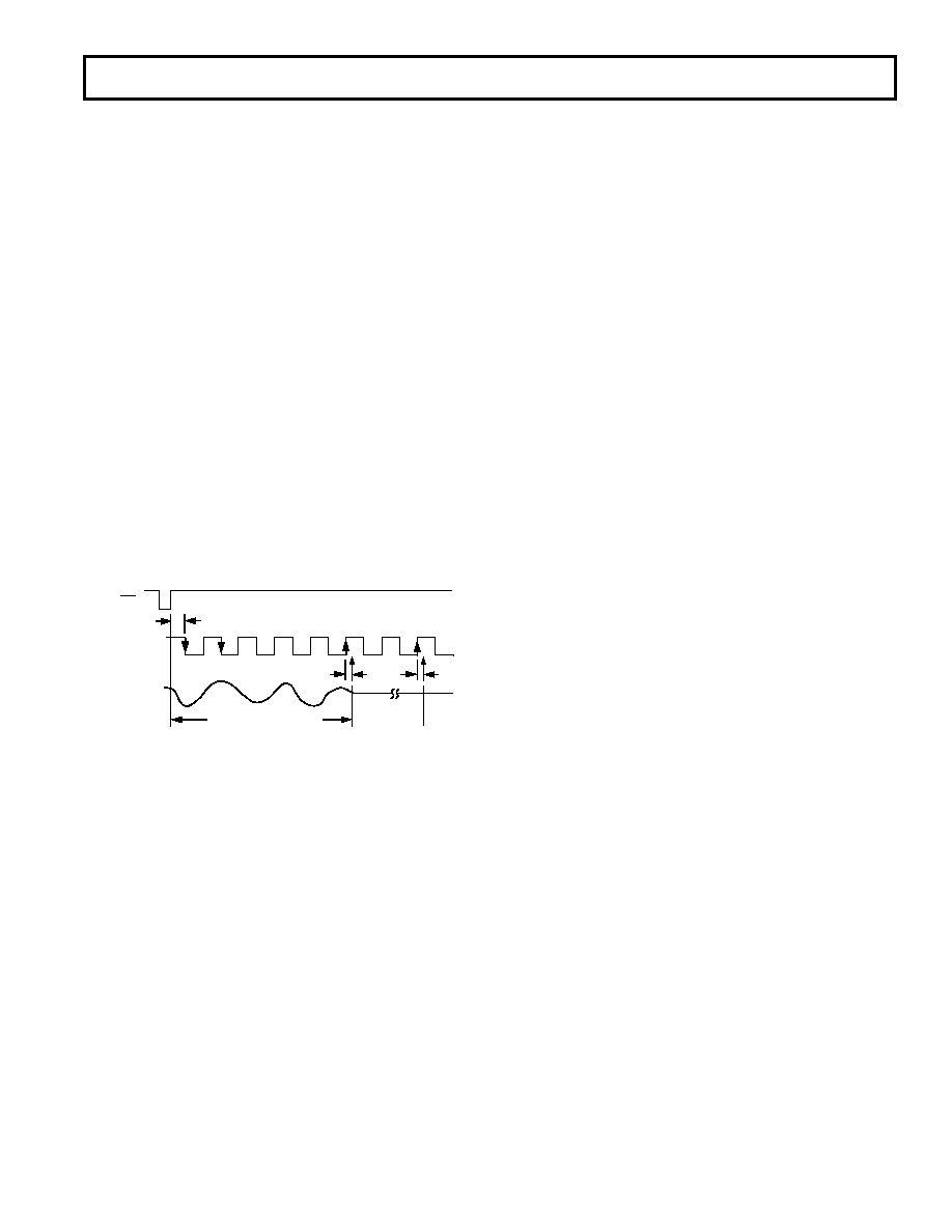
ADC Conversion Start Timing
Figure 6 shows the operating waveforms for the start of a conver-
sion cycle. On the rising edge of
WR, the conversion cycle starts
with the acquisition and tracking of the selected ADC channel,
AIN1–8. The analog input voltage is held 40 ns (typically) after
the first rising edge of CLKIN following four complete CLKIN
cycles. If tD in Figure 6 is greater than 12 ns, the falling edge of
CLKIN as shown is seen as the first falling clock edge. If tD is
less than 12 ns, the first falling clock edge to be recognized does
not occur until one cycle later.
Following the “hold” on the analog input(s), two complete
CLKIN cycles are allowed for settling purposes before the MSB
decision is made. The actual decision point occurs approximately
40 ns after the rising edge of CLKIN as shown in Figure 6. Two
more CLKIN cycles are allowed for the second MSB decision.
The succeeding bit decisions are made approximately 40 ns
after each rising edge of CLKIN until the conversion is complete.
At the end of conversion, if a single conversion has been
requested (CR6 = 0), the
BUSY/INT line changes state (as
programmed by CR9) and the SAR contents are transferred to
the first register ADCREG1. The SAR is then reset in readiness for
a new conversion. If simultaneous sampling has been requested
(CR6 = 1), no change occurs in the status of the
BUSY/INT
output, and the ADC automatically starts the second conversion.
At the end of this conversion, the
BUSY/INT line changes state
(as programmed by CR9) and the SAR contents are transferred
to the second register, ADCREG2.
tD*
CLKIN
VIN
WR
CHANNEL ACQUISITION
40ns
TYP
40ns
TYP
'HOLD'
DB9 (MSB)
* TIMING SHOWN FOR tD GREATER THAN 12ns
Figure 6. ADC Conversion Start Timing
Track-and-Hold
The track-and-hold (T/H) amplifiers on the analog input(s) of
the AD7776/AD7777/AD7778 allow the ADC to accurately
convert an input sine wave of 2 V peak-peak amplitude up to a
frequency of 189 kHz, the Nyquist frequency of the ADC when
operated at its maximum throughput rate of 378 kHz. This
maximum rate of conversion includes conversion time and the
time between conversions. Because the input bandwidth of the
track-and-hold is much greater than 189 kHz, the input signal
should be band limited to avoid folding unwanted signals into
the band of interest.
Power-Down
The AD7776/AD7777/AD7778 can be placed in a power-down
mode simply by writing a logic high to location CR8 of the
control register. The following changes are effected immediately
upon writing a “1” to location CR8:
Any conversion in progress is terminated.
If a conversion is in progress, the leading edge of WR immedi-
ately drives the
BUSY/INT output high.
All the linear circuitry is turned off.
The REFOUT output stops being driven and is weakly (5 k)
pulled to analog ground.
Control inputs
CS, WR, and RD retain their purpose while the
AD7776/AD7777/AD7778 is in power-down mode. If no
conversions are in progress when the AD7776/AD7777/AD7778
is placed into power-down mode, the contents of the ADC
registers, ADCREG1 and ADCREG2, are retained during
power-down and can be read as normal. On returning to normal
operating mode, a new conversion (or conversions, dependent
on CR6) is automatically started. Upon completion, the invalid
conversion results are loaded into the ADC registers, losing the
previous valid results.
To achieve the lowest possible power consumption in the
power-down mode, special attention must be paid to the state of
the digital and analog inputs and outputs:
Because each analog input channel sees a resistive divider to
AGND, the input resistance of which does not change
between normal and power-down modes, driving the analog
input signals to 0 V or as close as possible to 0 V minimizes
the power dissipated in the input signal conditioning circuitry.
Similarly, the REFIN input sees a resistive divider to AGND,
the input resistance of which does not change between
normal and power-down modes. If an external reference is
being used, then driving this reference input to 0 V or as
close as possible to 0 V minimizes the power dissipated in
the input signal conditioning circuitry.
Since the REFOUT pin is pulled to AGND via, typically, a
5 k
resistor, any voltage above 0 V that this output may be
pulled to by external circuitry dissipates unnecessary power.
Digital inputs CS, WR, and RD should all be held at V
CC or
as close as possible. CLKIN should be held as close as
possible to either 0 V or VCC.
Since the BUSY/INT output is actively driven to a logic high,
any loading on this pin to 0 V dissipates power.
The AD7776/AD7777/AD7778 comes out of the power-down
mode when a Logic “0” is written to location CR8 of the
control register. Note that the contents of the other locations
in the control register are retained when the device is placed in
power-down and are valid when power is restored. However,
coming out of power-down provides an opportunity to reload
the complete contents of the control register without any
extra instructions.
相关PDF资料 |
PDF描述 |
|---|---|
| VI-223-IW-F4 | CONVERTER MOD DC/DC 24V 100W |
| LTC2247IUH#TRPBF | IC ADC 14BIT 40MSPS SAMPL 32-QFN |
| VI-223-IW-F2 | CONVERTER MOD DC/DC 24V 100W |
| VE-BN0-MW-F2 | CONVERTER MOD DC/DC 5V 100W |
| AD7858BR | IC ADC 12BIT 8CH SRL 24-SOIC |
相关代理商/技术参数 |
参数描述 |
|---|---|
| AD7779ACPZ | 功能描述:24 Bit Analog to Digital Converter 8 Input 8 Sigma-Delta 64-LFCSP (9x9) 制造商:analog devices inc. 系列:- 包装:托盘 零件状态:有效 位数:24 采样率(每秒):16k 输入数:8 输入类型:差分,单端 数据接口:串行 配置:PGA-ADC 无线电 - S/H:ADC:- A/D 转换器数:8 架构:三角积分 参考类型:外部, 内部 电压 - 电源,模拟:±1.65V,2.2 V ~ 3.6 V 电压 - 电源,数字:- 特性:同步采样 工作温度:-40°C ~ 125°C 封装/外壳:64-WFQFN 裸露焊盘 供应商器件封装:64-LFCSP(9x9) 标准包装:1 |
| AD7779ACPZ-RL | 功能描述:IC ADC 24BIT 16KSPS 制造商:analog devices inc. 系列:* 零件状态:有效 标准包装:2,500 |
| AD7780 | 制造商:AD 制造商全称:Analog Devices 功能描述:24-Bit, Pin-Programmable, Ultralow Power Sigma-Delta ADC |
| AD7780BRUZ | 功能描述:IC ADC 24BIT 1CH LP SD 16TSSOP RoHS:是 类别:集成电路 (IC) >> 数据采集 - 模数转换器 系列:- 标准包装:1 系列:microPOWER™ 位数:8 采样率(每秒):1M 数据接口:串行,SPI? 转换器数目:1 功率耗散(最大):- 电压电源:模拟和数字 工作温度:-40°C ~ 125°C 安装类型:表面贴装 封装/外壳:24-VFQFN 裸露焊盘 供应商设备封装:24-VQFN 裸露焊盘(4x4) 包装:Digi-Reel® 输入数目和类型:8 个单端,单极 产品目录页面:892 (CN2011-ZH PDF) 其它名称:296-25851-6 |
| AD7780BRUZ-REEL | 功能描述:IC ADC 24BIT 1CH LP SD 16TSSOP RoHS:是 类别:集成电路 (IC) >> 数据采集 - 模数转换器 系列:- 标准包装:2,500 系列:- 位数:16 采样率(每秒):15 数据接口:MICROWIRE?,串行,SPI? 转换器数目:1 功率耗散(最大):480µW 电压电源:单电源 工作温度:-40°C ~ 85°C 安装类型:表面贴装 封装/外壳:38-WFQFN 裸露焊盘 供应商设备封装:38-QFN(5x7) 包装:带卷 (TR) 输入数目和类型:16 个单端,双极;8 个差分,双极 配用:DC1011A-C-ND - BOARD DELTA SIGMA ADC LTC2494 |
发布紧急采购,3分钟左右您将得到回复。