参数资料
| 型号: | AD7780BRZ-REEL |
| 厂商: | Analog Devices Inc |
| 文件页数: | 14/16页 |
| 文件大小: | 0K |
| 描述: | IC ADC 24BIT 1CH LP SD 14SOIC |
| 设计资源: | Weigh Scale Design Using AD7780 with Internal PGA (CN0107) |
| 标准包装: | 2,500 |
| 位数: | 24 |
| 采样率(每秒): | 16.7 |
| 数据接口: | 串行,SPI? |
| 转换器数目: | 1 |
| 电压电源: | 模拟和数字 |
| 工作温度: | -40°C ~ 105°C |
| 安装类型: | 表面贴装 |
| 封装/外壳: | 14-SOIC(0.154",3.90mm 宽) |
| 供应商设备封装: | 14-SO |
| 包装: | 带卷 (TR) |
| 输入数目和类型: | 1 个差分,双极 |
AD7780
Rev. A | Page 7 of 16
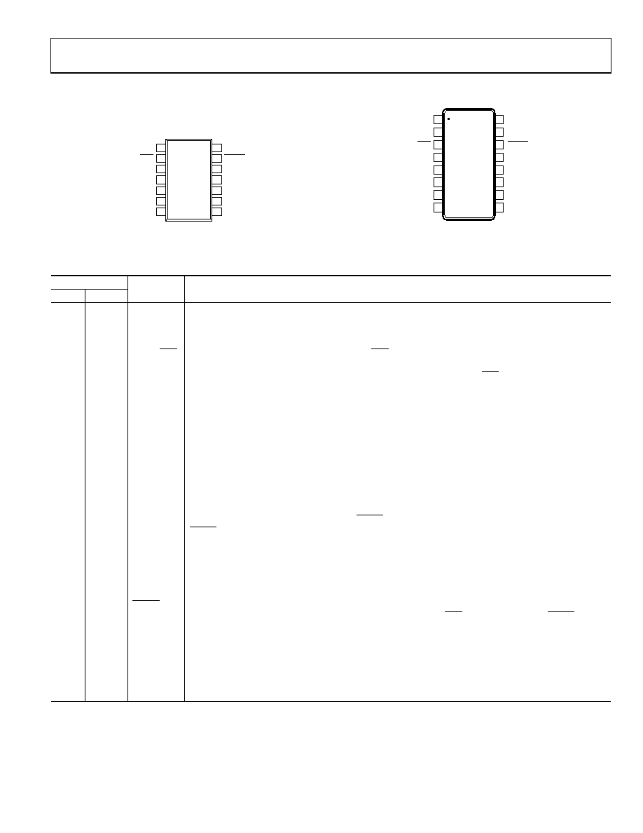
PIN CONFIGURATIONS AND FUNCTION DESCRIPTIONS
AD7780
TOP VIEW
(Not to Scale)
NC = NO CONNECT
1
2
3
4
5
6
7
8
SCLK
DOUT/RDY
NC
AIN(–)
AIN(+)
GAIN
NC
REFIN(+)
16
15
14
13
12
11
10
9
FILTER
PDRST
DVDD
BPDSW
REFIN(–)
GND
AVDD
NC
0
794
5-
0
07
SCLK 1
DOUT/RDY 2
NC 3
GAIN 4
FILTER
14
PDRST
13
DVDD
12
AVDD
11
AIN(+) 5
GND
10
AIN(–) 6
BPDSW
9
REFIN(+) 7
REFIN(–)
8
AD7780
TOP VIEW
(Not to Scale)
NC = NO CONNECT
0
79
45
-0
06
Figure 6. SOIC Pin Configuration
Figure 7. TSSOP Pin Configuration
Table 6. Pin Function Descriptions
Pin No.
SOIC
TSSOP
Mnemonic
Description
1
2
SCLK
Serial Clock Input. This serial clock input is for data transfers from the ADC. The SCLK pin has a Schmitt-
triggered input. The serial clock can be active only when transferring data from the AD7780. The data
from the AD7780 can be read as a continuous 32-bit word. Alternatively, SCLK can be noncontinuous
during the data transfer, with the information being transmitted from the ADC in smaller data batches.
2
3
DOUT/RDY
Serial Data Output/Data Ready Output. DOUT/RDY serves a dual purpose: as a data ready pin, going low to
indicate the completion of a conversion, and as a serial data output pin to access the data register of the
ADC. Eight status bits accompany each data read (see
). The DOUT/
RDY falling edge can be used
as an interrupt to a processor, indicating that new data is available. If the data is not read after the conver-
sion, the pin goes high before the next update occurs. The serial interface is reset each time that a conversion is
available. Therefore, the user must ensure that any conversions being transmitted are completed before
the next conversion is available.
3
1, 4, 16
NC
No Connect. This pin can be left floating.
4
5
GAIN
Gain Select Pin. When GAIN is low, the gain is set to 128. When GAIN is high, the gain is set to 1.
5
6
AIN(+)
Analog Input. AIN(+) is the positive terminal of the differential analog input pair, AIN(+)/AIN().
6
7
AIN()
Analog Input. AIN() is the negative terminal of the differential analog input pair, AIN(+)/AIN().
7
8
REFIN(+)
Positive Reference Input. An external reference can be applied between REFIN(+) and REFIN(). The nomi-
nal reference voltage (REFIN(+) REFIN()) is 5 V, but the part can function with a reference of 0.5 V to AVDD.
8
9
REFIN()
Negative Reference Input.
9
10
BPDSW
Bridge Power-Down Switch to GND. When PDRST is high, the bridge power-down switch is closed. When
PDRST is low, the switch is opened.
10
11
GND
Ground Reference Point.
11
12
AVDD
Supply Voltage, 2.7 V to 5.25 V.
12
13
DVDD
Digital Interface Supply Voltage. The logic levels for the serial interface pins and the digital control pins
are related to this supply, which is between 2.7 V and 5.25 V. The DVDD voltage is independent of the
voltage on AVDD; therefore, AVDD can equal 5 V with DVDD at 3 V or vice versa.
13
14
PDRST
Power-Down/Reset. When this pin is low, the ADC is placed in power-down mode, and the low-side power
switch is opened. All the logic on the chip is reset, and the DOUT/RDY pin is tristated. When PDRST is high,
the ADC is taken out of power-down mode. The on-chip clock powers up and settles, and the ADC
continuously converts. In addition, the low-side power switch is closed. The internal clock requires
approximately 1 ms to power up.
14
15
FILTER
Filter Select. When FILTER is low, the fast settling filter is selected. The update rate is set to 16.7 Hz, which
gives a filter settling time of 120 ms. When FILTER is high, the high rejection filter is selected. The update
rate is set to 10 Hz, which gives a filter settling time of 300 ms. With this filter, the stop-band (higher than
fADC) attenuation is better than 45 dB.
相关PDF资料 |
PDF描述 |
|---|---|
| AD7781CRZ | IC ADC 20BIT 1CH LP SD 14SOIC |
| AD7782BRUZ | IC ADC 24BIT 2CHAN 16TSSOP |
| AD7783BRU | IC ADC 24BIT 2CH R-R 16-TSSOP |
| AD7785BRUZ-REEL | IC ADC 20BIT 3CH LN LP 16-TSSOP |
| AD7787BRMZ | IC ADC 24BIT 2CH LP SIG 10MSOP |
相关代理商/技术参数 |
参数描述 |
|---|---|
| AD7781 | 制造商:AD 制造商全称:Analog Devices 功能描述:20-Bit, Pin-Programmable, Low Power Sigma-Delta ADC |
| AD7781BRUZ | 功能描述:IC ADC 20BIT 1CH LP SD 16TSSOP RoHS:是 类别:集成电路 (IC) >> 数据采集 - 模数转换器 系列:- 标准包装:1 系列:microPOWER™ 位数:8 采样率(每秒):1M 数据接口:串行,SPI? 转换器数目:1 功率耗散(最大):- 电压电源:模拟和数字 工作温度:-40°C ~ 125°C 安装类型:表面贴装 封装/外壳:24-VFQFN 裸露焊盘 供应商设备封装:24-VQFN 裸露焊盘(4x4) 包装:Digi-Reel® 输入数目和类型:8 个单端,单极 产品目录页面:892 (CN2011-ZH PDF) 其它名称:296-25851-6 |
| AD7781BRUZ-REEL | 功能描述:IC ADC 20BIT 1CH LP SD 16TSSOP RoHS:是 类别:集成电路 (IC) >> 数据采集 - 模数转换器 系列:- 标准包装:2,500 系列:- 位数:16 采样率(每秒):15 数据接口:MICROWIRE?,串行,SPI? 转换器数目:1 功率耗散(最大):480µW 电压电源:单电源 工作温度:-40°C ~ 85°C 安装类型:表面贴装 封装/外壳:38-WFQFN 裸露焊盘 供应商设备封装:38-QFN(5x7) 包装:带卷 (TR) 输入数目和类型:16 个单端,双极;8 个差分,双极 配用:DC1011A-C-ND - BOARD DELTA SIGMA ADC LTC2494 |
| AD7781BRZ | 功能描述:IC ADC 20BIT 1CH LP SD 14SOIC RoHS:是 类别:集成电路 (IC) >> 数据采集 - 模数转换器 系列:- 标准包装:1,000 系列:- 位数:16 采样率(每秒):45k 数据接口:串行 转换器数目:2 功率耗散(最大):315mW 电压电源:模拟和数字 工作温度:0°C ~ 70°C 安装类型:表面贴装 封装/外壳:28-SOIC(0.295",7.50mm 宽) 供应商设备封装:28-SOIC W 包装:带卷 (TR) 输入数目和类型:2 个单端,单极 |
| AD7781BRZ | 制造商:Analog Devices 功能描述:IC ADC 20BIT 16.7SPS SOIC-14 |
发布紧急采购,3分钟左右您将得到回复。