- 您现在的位置:买卖IC网 > PDF目录10309 > AD7782BRUZ-REEL7 (Analog Devices Inc)IC ADC 24BIT 2CHAN 16TSSOP PDF资料下载
参数资料
| 型号: | AD7782BRUZ-REEL7 |
| 厂商: | Analog Devices Inc |
| 文件页数: | 9/12页 |
| 文件大小: | 0K |
| 描述: | IC ADC 24BIT 2CHAN 16TSSOP |
| 标准包装: | 1,000 |
| 位数: | 24 |
| 采样率(每秒): | 19.79 |
| 数据接口: | DSP,MICROWIRE?,QSPI?,串行,SPI? |
| 转换器数目: | 1 |
| 功率耗散(最大): | 3.9mW |
| 电压电源: | 单电源 |
| 工作温度: | -40°C ~ 85°C |
| 安装类型: | 表面贴装 |
| 封装/外壳: | 16-TSSOP(0.173",4.40mm 宽) |
| 供应商设备封装: | 16-TSSOP |
| 包装: | 带卷 (TR) |
| 输入数目和类型: | 2 个差分,单极;2 个差分,双极 |
AD7782
–6–
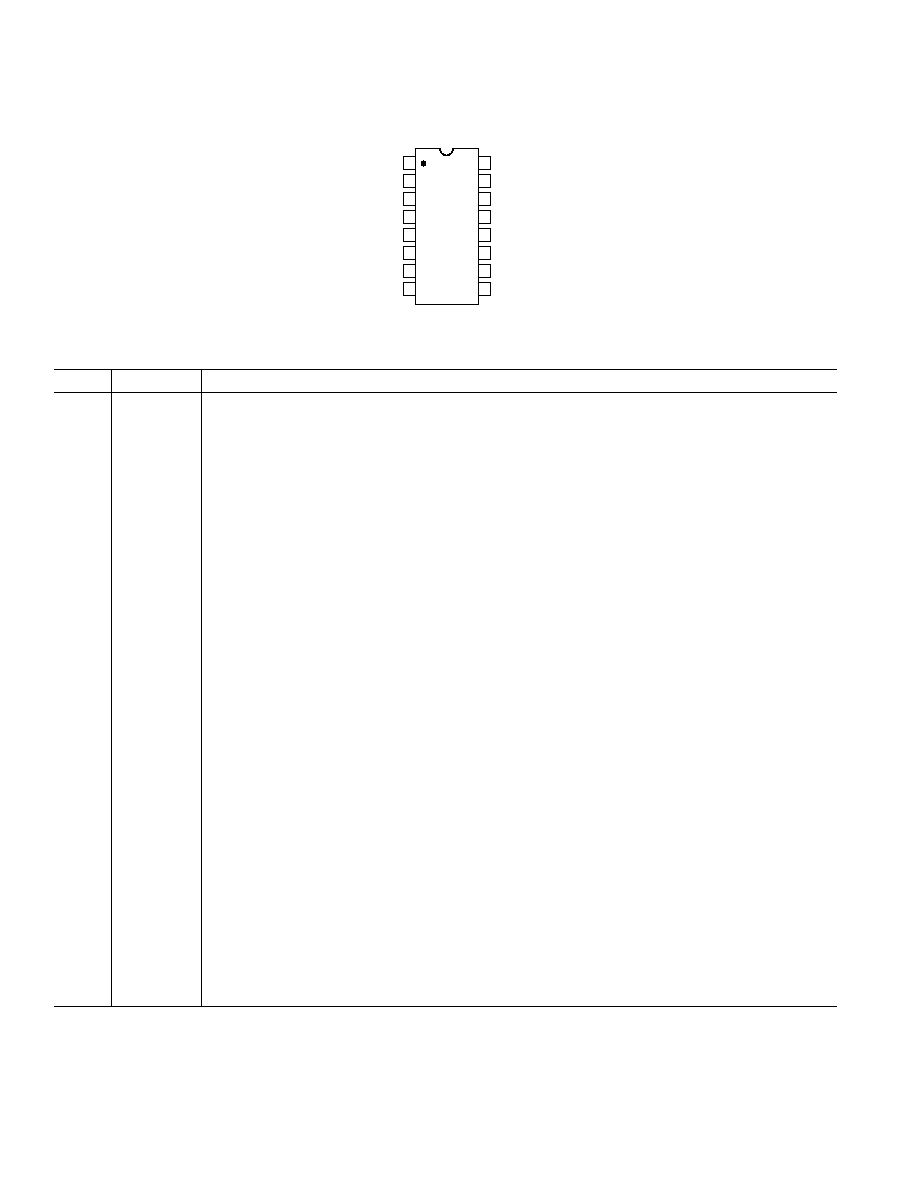
PIN CONFIGURATION
TOP VIEW
(Not to Scale)
XTAL1
AD7782
REFIN(+)
REFIN(–)
AIN1(+)
AIN1(–)
AIN2(+)
AIN2(–)
CH1/CH2
XTAL2
VDD
GND
MODE
DOUT/
RDY
CS
SCLK
RANGE
1
2
3
4
5
6
7
8
16
15
14
13
12
11
10
9
PIN FUNCTION DESCRIPTIONS
Pin No.
Mnemonic
Function
1
XTAL1
Input to the 32.768 kHz Crystal Oscillator Inverter.
2
REFIN(+)
Positive Reference Input. REFIN(+) can lie anywhere between VDD and GND +1 V. The nominal reference
voltage (REFIN(+) – REFIN(–)) is 2.5 V, but the part functions with a reference from 1 V to VDD.
3
REFIN(–)
Negative Reference Input. This reference input can lie anywhere between GND and VDD – 1 V.
4
AIN1(+)
Analog Input. AIN1(+) is the positive terminal of the fully-differential analog input pair AIN1(+)/AIN1(–).
5
AIN1(–)
Analog Input. AIN1(–) is the negative terminal of the fully-differential analog input pair AIN1(+)/AIN1(–).
6
AIN2(+)
Analog Input. AIN2(+) is the positive terminal of the fully-differential analog input pair AIN2(+)/AIN2(–).
7
AIN2(–)
Analog Input. AIN2(–) is the negative terminal of the fully-differential analog input pair AIN2(+)/AIN2(–).
8
CH1/CH2
Channel Select, Logic Input. With
CH1/CH2 = 0, channel AIN1(+)/AIN1(–) is selected while the active
channel is AIN2(+)/AIN2(–) when
CH1/CH2 = 1.
9
RANGE
Logic Input which configures the input range on the internal PGA. With RANGE = 0, the full-scale input
range is
±160 mV while the full-scale input range equals ±2.56 V when RANGE = 1 for a +2.5 V Reference.
10
SCLK
Serial Clock Input/Output for Data Transfers from the ADC. When the device is operated in master mode,
SCLK is an output with one SCLK period equal to one XTAL period. In slave mode, SCLK is generated
by an external source. In slave mode, all the data can be transmitted on a continuous train of pulses.
Alternatively, SCLK can be a noncontinuous clock with the information being transmitted from the AD7782
in smaller batches of data. SCLK is Schmitt triggered (slave mode) making the interface suitable for opto-
isolated applications.
11
CS
Chip Select Input.
CS is an active low logic input used to select the AD7782. When CS is low, the PLL
establishes lock and allows the AD7782 to initiate a conversion on the selected channel. When
CS is high,
the conversion is aborted, DOUT and SCLK are three-stated, the AD7782 enters standby mode and any
conversion result in the output shift register is lost.
12
DOUT/
RDY Serial Data Output/Data Ready Output. DOUT/RDY serves a dual purpose in this interface. When a con-
version is initiated, DOUT/
RDY goes high and remains high until the conversion is complete. DOUT/RDY
will then return low to indicate that valid data is available to be read from the device. In slave mode, this acts
as an interrupt to the processor indicating that valid data is available. If data is not read after a conversion,
DOUT/
RDY will go high before the next update occurs. In master mode, DOUT/RDY goes low for at least
half an SCLK cycle before the device produces SCLKs. When SCLK becomes active, data is output on
the DOUT/
RDY pin. Data is output on the falling SCLK edge and is valid on the rising edge.
13
MODE
The MODE pin selects master or slave mode of operation. When MODE = 0, the AD7782 operates in
master mode while the AD7782 is configured for slave mode when MODE = 1.
14
GND
Ground Reference Point for the AD7782.
15
VDD
Supply Voltage, 3 V or 5 V Nominal.
16
XTAL2
Output from the 32.768 kHz Crystal Oscillator Inverter.
REV. A
相关PDF资料 |
PDF描述 |
|---|---|
| MS27472T12F4PA | CONN RCPT 4POS WALL MT W/PINS |
| VE-B42-MW-S | CONVERTER MOD DC/DC 15V 100W |
| D38999/24FG41BN | CONN HSG RCPT 41POS JAM NUT SCKT |
| VI-22W-MY | CONVERTER MOD DC/DC 5.5V 50W |
| VI-22T-MY | CONVERTER MOD DC/DC 6.5V 50W |
相关代理商/技术参数 |
参数描述 |
|---|---|
| AD7783 | 制造商:AD 制造商全称:Analog Devices 功能描述:Read-Only, Pin Configured 24-Bit ADC with Excitation Current Sources |
| AD7783BRU | 功能描述:IC ADC 24BIT 2CH R-R 16-TSSOP RoHS:否 类别:集成电路 (IC) >> 数据采集 - 模数转换器 系列:- 标准包装:1,000 系列:- 位数:16 采样率(每秒):45k 数据接口:串行 转换器数目:2 功率耗散(最大):315mW 电压电源:模拟和数字 工作温度:0°C ~ 70°C 安装类型:表面贴装 封装/外壳:28-SOIC(0.295",7.50mm 宽) 供应商设备封装:28-SOIC W 包装:带卷 (TR) 输入数目和类型:2 个单端,单极 |
| AD7783BRU-REEL | 功能描述:IC ADC 24BIT 2CH R-R 16-TSSOP RoHS:否 类别:集成电路 (IC) >> 数据采集 - 模数转换器 系列:- 标准包装:1,000 系列:- 位数:16 采样率(每秒):45k 数据接口:串行 转换器数目:2 功率耗散(最大):315mW 电压电源:模拟和数字 工作温度:0°C ~ 70°C 安装类型:表面贴装 封装/外壳:28-SOIC(0.295",7.50mm 宽) 供应商设备封装:28-SOIC W 包装:带卷 (TR) 输入数目和类型:2 个单端,单极 |
| AD7783BRU-REEL7 | 功能描述:IC ADC 24BIT 2CH R-R 16-TSSOP RoHS:否 类别:集成电路 (IC) >> 数据采集 - 模数转换器 系列:- 标准包装:1,000 系列:- 位数:16 采样率(每秒):45k 数据接口:串行 转换器数目:2 功率耗散(最大):315mW 电压电源:模拟和数字 工作温度:0°C ~ 70°C 安装类型:表面贴装 封装/外壳:28-SOIC(0.295",7.50mm 宽) 供应商设备封装:28-SOIC W 包装:带卷 (TR) 输入数目和类型:2 个单端,单极 |
| AD7783BRUZ | 功能描述:IC ADC 24BIT SGL R-R 16-TSSOP RoHS:是 类别:集成电路 (IC) >> 数据采集 - 模数转换器 系列:- 标准包装:1 系列:microPOWER™ 位数:8 采样率(每秒):1M 数据接口:串行,SPI? 转换器数目:1 功率耗散(最大):- 电压电源:模拟和数字 工作温度:-40°C ~ 125°C 安装类型:表面贴装 封装/外壳:24-VFQFN 裸露焊盘 供应商设备封装:24-VQFN 裸露焊盘(4x4) 包装:Digi-Reel® 输入数目和类型:8 个单端,单极 产品目录页面:892 (CN2011-ZH PDF) 其它名称:296-25851-6 |
发布紧急采购,3分钟左右您将得到回复。