- 您现在的位置:买卖IC网 > PDF目录10254 > AD7787BRM (Analog Devices Inc)IC ADC 24BIT LP 2CH SIG 10-MSOP PDF资料下载
参数资料
| 型号: | AD7787BRM |
| 厂商: | Analog Devices Inc |
| 文件页数: | 11/20页 |
| 文件大小: | 0K |
| 描述: | IC ADC 24BIT LP 2CH SIG 10-MSOP |
| 标准包装: | 50 |
| 位数: | 24 |
| 采样率(每秒): | 120 |
| 数据接口: | DSP,MICROWIRE?,QSPI?,串行,SPI? |
| 转换器数目: | 1 |
| 功率耗散(最大): | 225µW |
| 电压电源: | 单电源 |
| 工作温度: | -40°C ~ 105°C |
| 安装类型: | 表面贴装 |
| 封装/外壳: | 10-TFSOP,10-MSOP(0.118",3.00mm 宽) |
| 供应商设备封装: | 10-MSOP |
| 包装: | 管件 |
| 输入数目和类型: | 1 个单端,单极;1 个单端,双极;1 个差分,单极;1 个差分,双极 |
Data Sheet
AD7787
Rev. A | Page 19 of 20
Reference voltage sources like those previously recommended,
e.g., ADR391, will typically have low output impedances and
are, therefore, tolerant to having decoupling capacitors on
REFIN without introducing gain errors in the system. Deriving
the reference input voltage across an external resistor means
that the reference input sees a significant external source
impedance. External decoupling on the REFIN pin is not
recommended in this type of circuit configuration.
VDD MONITOR
Along with converting external voltages, the AD7787 can
monitor the voltage on the VDD pin. When the CH1 and CH0
bits in the communications register are set to 1, the voltage on
the VDD pin is internally attenuated by 5 and the resultant
voltage is applied to the Σ-Δ modulator using an internal
1.17 V reference for the analog-to-digital conversion. This is
useful because variations in the power supply voltage can be
monitored.
GROUNDING AND LAYOUT
The digital filter provides rejection of broadband noise on the
power supply, except at integer multiples of the modulator
sampling frequency. The digital filter also removes noise from
the analog and reference inputs, provided that these noise
sources do not saturate the analog modulator. As a result, the
AD7787 is more immune to noise interference than a
conventional high resolution converter. However, because the
resolution of the AD7787 is so high, and the noise levels from
the AD7787 are so low, care must be taken with regard to
grounding and layout.
The printed circuit board that houses the AD7787 should be
designed such that the analog and digital sections are separated
and confined to certain areas of the board. A minimum etch
technique is generally best for ground planes because it gives
the best shielding.
It is recommended that the AD7787’s GND pin be tied to the
AGND plane of the system. In any layout, it is important that
the user keep in mind the flow of currents in the system,
ensuring that the return paths for all currents are as close as
possible to the paths the currents took to reach their
destinations. Avoid forcing digital currents to flow through the
AGND sections of the layout.
The AD7787’s ground plane should be allowed to run under the
AD7787 to prevent noise coupling. The power supply lines to
the AD7787 should use as wide a trace as possible to provide
low impedance paths and reduce the effects of glitches on the
power supply line. Fast switching signals, such as clocks, should
be shielded with digital ground to avoid radiating noise to other
sections of the board, and clock signals should never be run
near the analog inputs. Avoid crossover of digital and analog
signals. Traces on opposite sides of the board should run at
right angles to each other. This reduces the effects of
feedthrough through the board. A microstrip technique is by far
the best, but it is not always possible with a double-sided board.
In this technique, the component side of the board is dedicated
to ground planes, while signals are placed on the solder side.
Good decoupling is important when using high resolution
ADCs. VDD should be decoupled with 10 μF tantalum in parallel
with 0.1 μF capacitors to GND. To achieve the best from these
decoupling components, they should be placed as close as
possible to the device, ideally right up against the device. All
logic chips should be decoupled with 0.1 μF ceramic capacitors
to DGND.
APPLICATIONS
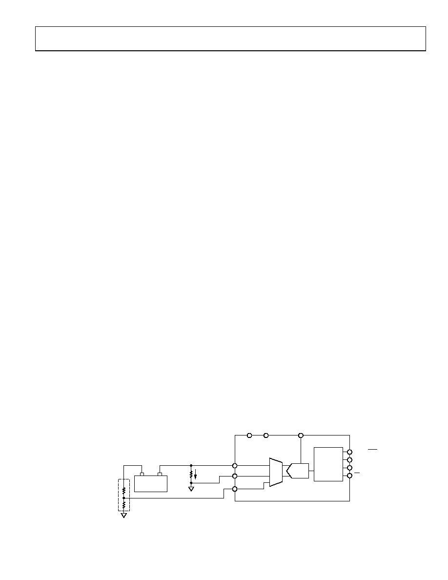
Battery Monitoring
In battery monitoring, the battery current and voltage are
measured. The current is passed through a 100 μΩ resistor.
Because the current is from 200 A to +2000 A, the result is a
voltage from 20 mV to +200 mV. Channel AIN1 of the
AD7787 can be connected directly to the shunt resistor to
measure this current. The battery voltage can vary from 12 V to
42 V with peaks up to 60 V. This voltage is attenuated using an
external resistor network before being applied to the AD7787.
The buffers onboard the AD7787 mean that channel AIN2 can
be connected directly to the high impedance attenuator circuit
without introducing gain errors.
04477-0-016
-
ADC
AIN1(–)
AIN1(+)
RSHUNT
100
–200A TO
+2000A
GND
REFIN
AD7787
VDD
DOUT/RDY
DIN
SCLK
CS
SERIAL
INTERFACE
AND
LOGIC
CONTROL
MUX
AIN2
12V OR 42V
(60V PEAK)
+
–
ATTENUATION
CIRCUIT
Figure 16. Battery Monitoring
相关PDF资料 |
PDF描述 |
|---|---|
| MS3101F28-3P | CONN RCPT 3POS FREE HNG W/PINS |
| LTC1418CG#TR | IC A/D CONV 14BIT SRL&PAR 28SSOP |
| CS5351-KSZ | IC ADC AUD 108DB 204KHZ 24-SOIC |
| LTC1418CG#TRPBF | IC A/D CONV 14BIT SRL&PAR 28SSOP |
| MS27467E15B18SA | CONN PLUG 18POS STRAIGHT W/SCKT |
相关代理商/技术参数 |
参数描述 |
|---|---|
| AD7787BRM-REEL | 功能描述:IC ADC 24BIT LP 2CH SIG 10-MSOP RoHS:否 类别:集成电路 (IC) >> 数据采集 - 模数转换器 系列:- 标准包装:1,000 系列:- 位数:16 采样率(每秒):45k 数据接口:串行 转换器数目:2 功率耗散(最大):315mW 电压电源:模拟和数字 工作温度:0°C ~ 70°C 安装类型:表面贴装 封装/外壳:28-SOIC(0.295",7.50mm 宽) 供应商设备封装:28-SOIC W 包装:带卷 (TR) 输入数目和类型:2 个单端,单极 |
| AD7787BRMZ | 功能描述:IC ADC 24BIT 2CH LP SIG 10MSOP RoHS:是 类别:集成电路 (IC) >> 数据采集 - 模数转换器 系列:- 标准包装:1,000 系列:- 位数:16 采样率(每秒):45k 数据接口:串行 转换器数目:2 功率耗散(最大):315mW 电压电源:模拟和数字 工作温度:0°C ~ 70°C 安装类型:表面贴装 封装/外壳:28-SOIC(0.295",7.50mm 宽) 供应商设备封装:28-SOIC W 包装:带卷 (TR) 输入数目和类型:2 个单端,单极 |
| AD7787BRMZ | 制造商:Analog Devices 功能描述:IC 24BIT ADC SMD 7787 MSOP10 |
| AD7787BRMZ-RL | 功能描述:IC ADC 24BIT 2CH LP SIG 10MSOP RoHS:是 类别:集成电路 (IC) >> 数据采集 - 模数转换器 系列:- 标准包装:1,000 系列:- 位数:16 采样率(每秒):45k 数据接口:串行 转换器数目:2 功率耗散(最大):315mW 电压电源:模拟和数字 工作温度:0°C ~ 70°C 安装类型:表面贴装 封装/外壳:28-SOIC(0.295",7.50mm 宽) 供应商设备封装:28-SOIC W 包装:带卷 (TR) 输入数目和类型:2 个单端,单极 |
| AD7788 | 制造商:AD 制造商全称:Analog Devices 功能描述:Low Power, 16-/24-Bit Sigma-Delta ADC |
发布紧急采购,3分钟左右您将得到回复。