参数资料
| 型号: | AD7799BRU |
| 厂商: | Analog Devices Inc |
| 文件页数: | 28/28页 |
| 文件大小: | 0K |
| 描述: | IC ADC 24BIT 3CH LP 16-TSSOP |
| 标准包装: | 1 |
| 位数: | 24 |
| 采样率(每秒): | 470 |
| 数据接口: | DSP,MICROWIRE?,QSPI?,串行,SPI? |
| 转换器数目: | 1 |
| 功率耗散(最大): | 2.5mW |
| 电压电源: | 模拟和数字 |
| 工作温度: | -40°C ~ 105°C |
| 安装类型: | 表面贴装 |
| 封装/外壳: | 16-TSSOP(0.173",4.40mm 宽) |
| 供应商设备封装: | 16-TSSOP |
| 包装: | 管件 |
| 输入数目和类型: | 3 个差分,单极;3 个差分,双极 |
| 配用: | EVAL-AD7799EBZ-ND - BOARD EVALUATION FOR AD7799 |
| 其它名称: | Q2161119 |
第1页第2页第3页第4页第5页第6页第7页第8页第9页第10页第11页第12页第13页第14页第15页第16页第17页第18页第19页第20页第21页第22页第23页第24页第25页第26页第27页当前第28页
Data Sheet
AD7798/AD7799
Rev. B | Page 9 of 28
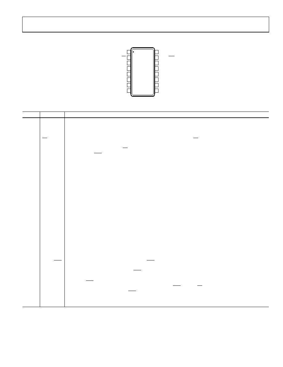
PIN CONFIGURATION AND FUNCTION DESCRIPTIONS
1
2
3
4
5
6
7
8
16
15
14
13
12
11
10
9
CS
AIN3(+)/P1
AIN3(–)/P2
AIN2(+)
AIN1(–)
AIN1(+)
SCLK
DOUT/RDY
DVDD
AVDD
REFIN(–)
AIN2(–)
REFIN(+)
PSW
GND
DIN
AD7798/
AD7799
TOP VIEW
(Not to Scale)
04856-
005
Figure 5. Pin Configuration
Table 4. Pin Function Descriptions
Pin No.
Mnemonic
Description
1
SCLK
Serial Clock Input. This serial clock input is for data transfers to and from the ADC. The SCLK has a Schmitt-triggered
input, making the interface suitable for opto-isolated applications. The serial clock can be continuous, with all data
transmitted in a continuous train of pulses. Alternatively, it can be noncontinuous, with the information transmitted
to or from the ADC in smaller batches of data.
2
CS
Chip Select Input. This is an active low logic input used to select the ADC. CS can be used to select the ADC in
systems with more than one device on the serial bus, or it can be used as a frame synchronization signal when
communicating with the device. CS can be hardwired low, allowing the ADC to operate in 3-wire mode, with SCLK,
DIN, and DOUT/RDY used to interface with the device.
3
AIN3(+)/P1
Analog Input/Digital Output Pin. AIN3(+) is the positive terminal of the differential analog input pair AIN3(+)/AIN3().
Alternatively, this pin can function as a general-purpose output bit referenced between AVDD and GND
4
AIN3()/P2
Analog Input/Digital Output Pin. AIN3() is the negative terminal of the differential analog input pair AIN3(+)/AIN3().
Alternatively, this pin can function as a general-purpose output bit referenced between AVDD and GND
5
AIN1(+)
Analog Input. AIN1(+) is the positive terminal of the differential analog input pair AIN1(+)/AIN1().
6
AIN1()
Analog Input. AIN1() is the negative terminal of the differential analog input pair AIN1(+)/AIN1().
7
AIN2(+)
Analog Input. AIN2(+) is the positive terminal of the differential analog input pair AIN2(+)/AIN2().
8
AIN2()
Analog Input. AIN2() is the negative terminal of the differential analog input pair AIN2(+)/AIN2().
9
REFIN(+)
Positive Reference Input. An external reference can be applied between REFIN(+) and REFIN(). REFIN(+) can lie
anywhere between AVDD and GND + 0.1 V. The nominal reference voltage (REFIN(+) – REFIN()) is 2.5 V, but the part
can function with a reference from 0.1 V to AVDD.
10
REFIN()
Negative Reference Input. REFIN() is the negative reference input for REFIN. This reference input can lie anywhere
between GND and AVDD 0.1 V.
11
PSW
Low-Side Power Switch to GND.
12
GND
Ground Reference Point.
13
AVDD
Supply Voltage. 2.7 V to 5.25 V.
14
DVDD
Digital Interface Supply Voltage. The logic levels for the serial interface pins are related to this supply, which is
between 2.7 V and 5.25 V. The DVDD voltage is independent of the voltage on AVDD; therefore, AVDD can equal 5 V
with DVDD at 3 V, or vice versa.
15
DOUT/RDY
Serial Data Output/Data Ready Output. DOUT/RDY serves a dual purpose. It functions as a serial data output pin to
access the output shift register of the ADC. The output shift register can contain data from any of the on-chip data
or control registers. In addition, DOUT/RDY operates as a data ready pin, going low to indicate the completion of a
conversion. If the data is not read after the conversion, the pin goes high before the next update occurs.
The DOUT/RDY falling edge can be used as an interrupt to a processor, indicating that valid data is available. With
an external serial clock, the data can be read using the DOUT/RDY pin. With CS low, the data/control word
information is placed on the DOUT/RDY pin on the SCLK falling edge and is valid upon the SCLK rising edge.
16
DIN
Serial Data Input to the Input Shift Register on the ADC. Data in this shift register is transferred to the control registers
within the ADC, with the register selection bits of the communication register identifying the appropriate register.
相关PDF资料 |
PDF描述 |
|---|---|
| AD7801BRU | IC DAC 8BIT PARALLEL INP 20TSSOP |
| AD7810YR | IC ADC 10BIT 2.7V 8-SOIC |
| AD7811YRZ-REEL7 | IC ADC 10BIT 4CHAN SRL 16SOIC |
| AD7813YRU | IC ADC 10BIT PARALLEL 16-TSSOP |
| AD7819YRZ-REEL7 | IC ADC 8BIT SAMPLING PAR 16SOIC |
相关代理商/技术参数 |
参数描述 |
|---|---|
| AD7799BRU-REEL | 功能描述:IC ADC 24BIT 3CH LP 16-TSSOP RoHS:否 类别:集成电路 (IC) >> 数据采集 - 模数转换器 系列:- 标准包装:1,000 系列:- 位数:16 采样率(每秒):45k 数据接口:串行 转换器数目:2 功率耗散(最大):315mW 电压电源:模拟和数字 工作温度:0°C ~ 70°C 安装类型:表面贴装 封装/外壳:28-SOIC(0.295",7.50mm 宽) 供应商设备封装:28-SOIC W 包装:带卷 (TR) 输入数目和类型:2 个单端,单极 |
| AD7799BRUZ | 功能描述:IC ADC 24BIT SIG-DEL 3CH 16TSSOP RoHS:是 类别:集成电路 (IC) >> 数据采集 - 模数转换器 系列:- 标准包装:1 系列:microPOWER™ 位数:8 采样率(每秒):1M 数据接口:串行,SPI? 转换器数目:1 功率耗散(最大):- 电压电源:模拟和数字 工作温度:-40°C ~ 125°C 安装类型:表面贴装 封装/外壳:24-VFQFN 裸露焊盘 供应商设备封装:24-VQFN 裸露焊盘(4x4) 包装:Digi-Reel® 输入数目和类型:8 个单端,单极 产品目录页面:892 (CN2011-ZH PDF) 其它名称:296-25851-6 |
| AD7799BRUZ-REEL | 功能描述:IC ADC 24BIT 3CH LP 16-TSSOP RoHS:是 类别:集成电路 (IC) >> 数据采集 - 模数转换器 系列:- 标准包装:1,000 系列:- 位数:16 采样率(每秒):45k 数据接口:串行 转换器数目:2 功率耗散(最大):315mW 电压电源:模拟和数字 工作温度:0°C ~ 70°C 安装类型:表面贴装 封装/外壳:28-SOIC(0.295",7.50mm 宽) 供应商设备封装:28-SOIC W 包装:带卷 (TR) 输入数目和类型:2 个单端,单极 |
| AD779AD | 制造商:AD 制造商全称:Analog Devices 功能描述:14-Bit 128 kSPS Complete Sampling ADC |
| AD779AJ | 制造商:未知厂家 制造商全称:未知厂家 功能描述:Analog-to-Digital Converter, 14-Bit |
发布紧急采购,3分钟左右您将得到回复。