参数资料
| 型号: | AD7808BR |
| 厂商: | Analog Devices Inc |
| 文件页数: | 28/28页 |
| 文件大小: | 0K |
| 描述: | IC DAC 10BIT 3.3V OCTAL 24-SOIC |
| 产品培训模块: | Data Converter Fundamentals DAC Architectures |
| 标准包装: | 31 |
| 设置时间: | 1.5µs |
| 位数: | 10 |
| 数据接口: | 串行 |
| 转换器数目: | 4 |
| 电压电源: | 模拟和数字 |
| 功率耗散(最大): | 99mW |
| 工作温度: | -40°C ~ 85°C |
| 安装类型: | 表面贴装 |
| 封装/外壳: | 24-SOIC(0.295",7.50mm 宽) |
| 供应商设备封装: | 24-SOIC W |
| 包装: | 管件 |
| 输出数目和类型: | 8 电压,双极 |
| 采样率(每秒): | 667k |
第1页第2页第3页第4页第5页第6页第7页第8页第9页第10页第11页第12页第13页第14页第15页第16页第17页第18页第19页第20页第21页第22页第23页第24页第25页第26页第27页当前第28页
AD7804/AD7805/AD7808/AD7809
–9–
REV. A
TERMINOLOGY
Relative Accuracy
For the DACs, relative accuracy or endpoint nonlinearity is a
measure of the maximum deviation, in LSBs, from a straight
line passing through the endpoints of the DAC transfer func-
tion. Figures 32 and 33 show the linearity at 3 V and 5 V
respectively.
Differential Nonlinearity
Differential nonlinearity is the difference between the measured
change and the ideal 1 LSB change between any two adjacent
codes. A specified differential nonlinearity of
±1 LSB maxi-
mum ensures monotonicity.
Bias Offset Error
If the DACs are ideal, the output voltage of any DAC with
midscale code loaded will be equal to VBIAS where VBIAS is se-
lected by MX1 and MX0 in the control register. The DAC bias
offset error is the difference between the actual output voltage
and VBIAS, expressed in mV.
Gain Error
The difference between the actual and ideal analog output
range, expressed as a percent of full-scale range. It is the devia-
tion in slope of the DAC transfer characteristic from ideal.
Zero-Scale Error
The zero-scale error is the actual output minus the ideal output
from any DAC when zero code is loaded to the DAC. If offset
binary coding is used, the code loaded is 000Hex, and if twos
complement coding is used, a code of 200HEX is loaded to the
DAC to calculate the zero-scale error. Zero-scale error is ex-
pressed in mV.
Digital-to-Analog Glitch Impulse
Digital-to-analog glitch impulse is the impulse injected into the
analog output when the digital inputs change state with the
DAC selected and the
LDAC used to update the DAC. It is
normally specified as the area of the glitch in nV-s and is mea-
sured when the digital input code is changed by 1 LSB at the
major carry transition. Regardless of whether offset binary or twos
complement coding is used, the major carry transition occurs at
the analog output voltage change of VBIAS to VBIAS – 1 LSB
or vice versa.
Digital Feedthrough
Digital feedthrough is a measure of the impulse injected into
the analog output of a DAC from the digital inputs of the same
DAC but is measured when the DAC is not updated. It is speci-
fied in nV secs and is measured with a full-scale code change on
the data bus, i.e., from all 0s to all 1s and vice versa.
Digital Crosstalk
Digital crosstalk is the glitch impulse transferred to the output
of one converter due to a digital code change to another DAC.
It is specified in nV-s.
Analog Crosstalk
Analog crosstalk is a change in output of any DAC in response
to a change in the output of one or more of the other DACs. It
is measured in LSBs.
Power Supply Rejection Ratio (PSRR)
This specification indicates how the output of the DAC is af-
fected by changes in the power supply voltage. Power-supply
rejection ratio is quoted in terms of % change in output per %
change in VDD for full-scale output of the DAC. VDD is varied
±10%.
AD7804/AD7808 INTERFACE SECTION
The AD7804 and AD7808 are serial input devices. Three lines
control the serial interface,
FSIN, CLKIN and SDIN. The timing
diagram is shown in Figure 1.
Two mode bits (MD1 and MD0) which are DB13 and DB14 of
the serial word written to the AD7804/AD7808 are used to deter-
mine whether writing is to the DAC data registers or the control
registers of the device. These parts contain a system control
register for controlling the operation of all DACs in the package
as well as a channel control register for controlling the operation of
each individual DAC. Table I shows how to access these registers.
Table I. Register Selection Table for the AD7804/AD7808
MD1
MD0
Function
0
Write enable to system control register.
0
1
Write enable to channel control register.
1
X
Write enable to DAC data registers.
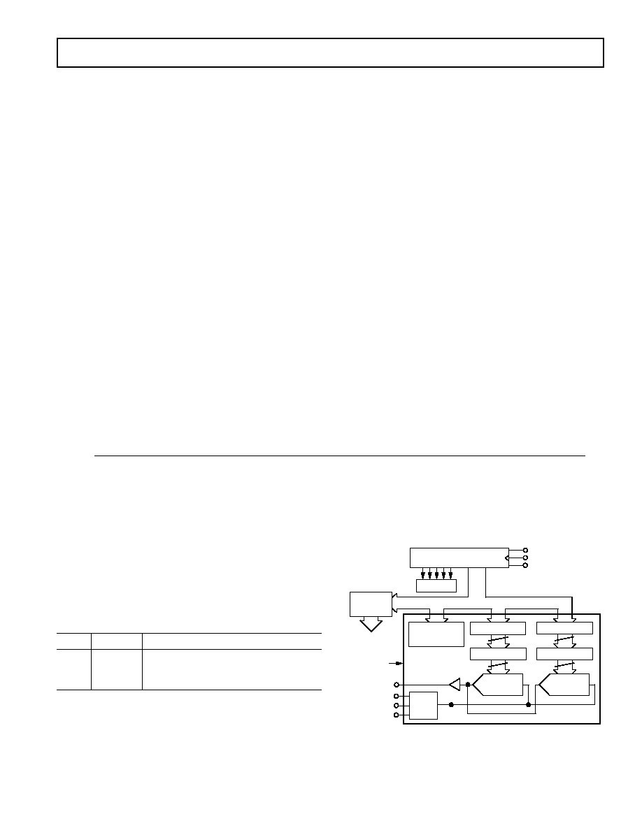
When the
FSIN input goes low, data appearing on the SDIN
line is clocked into the input register on each falling edge of
CLKIN. Data to be transferred to the AD7804/AD7808 is
loaded MSB first. Figure 4 shows the loading sequence for the
AD7804/AD7808 system control register, Figure 5 shows the
sequence for the channel control register write, and Figures 6
and 7 show the sequence for loading data to the Main and Sub
DAC data registers. Figure 3 shows the internal registers associ-
ated with the AD7804/AD7808 serial interface DACs. Only one
DAC structure is shown for clarity.
DATA REGISTER
8
VBIAS
INTERNAL VREF
VDD/2
REFIN
VOUT
FSIN
CLKIN
SDIN
TO ALL
CHANNELS
SINGLE
CHANNEL
DAC REGISTER
8
8-BIT DAC
(SUB DAC)
DATA REGISTER
10
DAC REGISTER
10
10-BIT DAC
(MAIN DAC)
CHANNEL
CONTROL
REGISTER
MUX
SYSTEM
CONTROL
REGISTER
16-BIT
INPUT SHIFT REGISTER
DECODER
Figure 3. AD7804/AD7808 Internal Registers
相关PDF资料 |
PDF描述 |
|---|---|
| AD7849CR | IC DAC 16BIT SRL INP 20-SOIC |
| AD7868BNZ | IC I/O PORT 12BIT ANLG 24-DIP |
| AD7869JRZ | IC I/O PORT 14BIT ANLG 28SOIC |
| AD7874SE | IC DAS 12BIT 4CH 5V 28-CLCC |
| AD7890BRZ-4 | IC DAS 12BIT 8CH 24-SOIC |
相关代理商/技术参数 |
参数描述 |
|---|---|
| AD7808BR-REEL | 功能描述:IC DAC 10BIT OCTAL SRL 24-SOIC RoHS:否 类别:集成电路 (IC) >> 数据采集 - 数模转换器 系列:- 产品培训模块:Data Converter Fundamentals DAC Architectures 标准包装:750 系列:- 设置时间:7µs 位数:16 数据接口:并联 转换器数目:1 电压电源:双 ± 功率耗散(最大):100mW 工作温度:0°C ~ 70°C 安装类型:表面贴装 封装/外壳:28-LCC(J 形引线) 供应商设备封装:28-PLCC(11.51x11.51) 包装:带卷 (TR) 输出数目和类型:1 电压,单极;1 电压,双极 采样率(每秒):143k |
| AD7808BRZ | 功能描述:IC DAC 10BIT OCTAL SRL 24-SOIC RoHS:是 类别:集成电路 (IC) >> 数据采集 - 数模转换器 系列:- 产品培训模块:Lead (SnPb) Finish for COTS Obsolescence Mitigation Program 标准包装:50 系列:- 设置时间:4µs 位数:12 数据接口:串行 转换器数目:2 电压电源:单电源 功率耗散(最大):- 工作温度:-40°C ~ 85°C 安装类型:表面贴装 封装/外壳:8-TSSOP,8-MSOP(0.118",3.00mm 宽) 供应商设备封装:8-uMAX 包装:管件 输出数目和类型:2 电压,单极 采样率(每秒):* 产品目录页面:1398 (CN2011-ZH PDF) |
| AD7808BRZ-REEL | 功能描述:IC DAC 10BIT OCTAL SRL 24-SOIC RoHS:是 类别:集成电路 (IC) >> 数据采集 - 数模转换器 系列:- 产品培训模块:Data Converter Fundamentals DAC Architectures 标准包装:750 系列:- 设置时间:7µs 位数:16 数据接口:并联 转换器数目:1 电压电源:双 ± 功率耗散(最大):100mW 工作温度:0°C ~ 70°C 安装类型:表面贴装 封装/外壳:28-LCC(J 形引线) 供应商设备封装:28-PLCC(11.51x11.51) 包装:带卷 (TR) 输出数目和类型:1 电压,单极;1 电压,双极 采样率(每秒):143k |
| AD7808BST | 制造商:AD 制造商全称:Analog Devices 功能描述:+3.3 V to +5 V Quad/Octal 10-Bit DACs(300.12 k) |
| AD7809 | 制造商:AD 制造商全称:Analog Devices 功能描述:+3.3 V to +5 V Quad/Octal 10-Bit DACs |
发布紧急采购,3分钟左右您将得到回复。