- 您现在的位置:买卖IC网 > PDF目录10322 > AD7812YRZ-REEL (Analog Devices Inc)IC ADC 10BIT 8CHAN SRL 20SOIC PDF资料下载
参数资料
| 型号: | AD7812YRZ-REEL |
| 厂商: | Analog Devices Inc |
| 文件页数: | 9/24页 |
| 文件大小: | 0K |
| 描述: | IC ADC 10BIT 8CHAN SRL 20SOIC |
| 标准包装: | 1,000 |
| 位数: | 10 |
| 采样率(每秒): | 350k |
| 数据接口: | DSP,串行 |
| 转换器数目: | 1 |
| 功率耗散(最大): | 10.5mW |
| 电压电源: | 单电源 |
| 工作温度: | -40°C ~ 105°C |
| 安装类型: | 表面贴装 |
| 封装/外壳: | 20-SOIC(0.295",7.50mm 宽) |
| 供应商设备封装: | 20-SOIC W |
| 包装: | 带卷 (TR) |
| 输入数目和类型: | 8 个单端,单极;7 伪差分,单极 |
AD7811/AD7812
–17–
REV. B
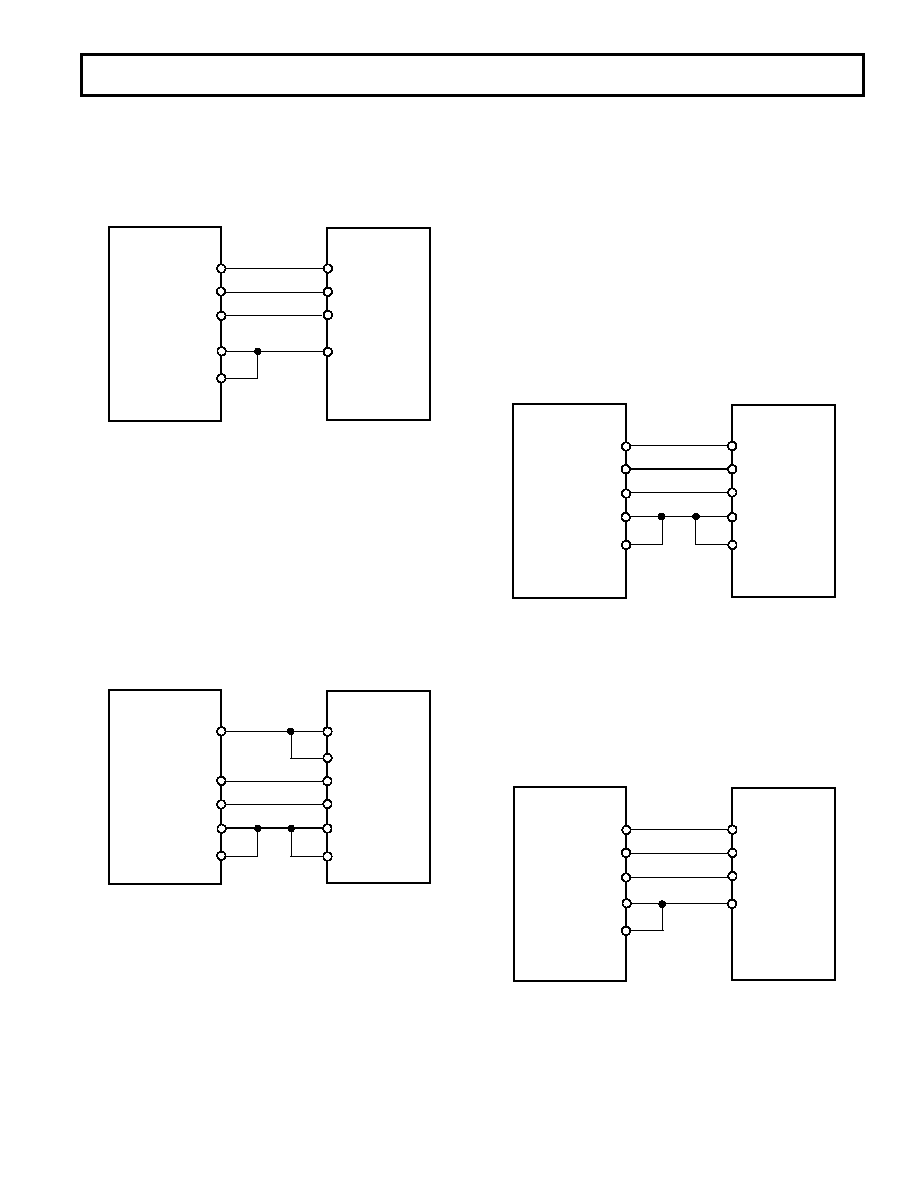
It is possible to implement a serial interface using the data ports
on the 8051. This would also allow a full duplex serial transfer
to be implemented. The technique involves “bit banging” an
I/O port (e.g., P1.0) to generate a serial clock and using two
other I/O ports (e.g., P1.1 and P1.2) to shift data in and out—
AD7811/AD7812*
DOUT
DIN
SCLK
RFS
TFS
8051*
P1.0
P1.1
P1.2
P1.3
*ADDITIONAL PINS OMITTED FOR CLARITY
Figure 22. Interfacing to the 8051 Using I/O Ports
AD7811/AD7812 to TMS320C5x
The serial interface on the TMS320C5x uses a continuous
serial clock and frame synchronization signals to synchronize
the data transfer operations with peripheral devices like the
AD7811. Frame synchronization inputs have been supplied on
the AD7811/AD7812 to allow easy interfacing with no extra
gluing logic. The serial port of the TMS320C5x is set up to
operate in Burst Mode with internal CLKX (Tx serial clock)
and FSX (Tx frame sync). The Serial Port Control register
(SPC) must have the following setup: F0 = 0, FSM = 1,
MCM = 1 and TXM = 1. The connection diagram is shown
in Figure 23.
AD7811/AD7812*
DOUT
SCLK
RFS
TFS
TMS320C5x*
CLKX
CLKR
FSX
*ADDITIONAL PINS OMITTED FOR CLARITY
FSR
DR
DIN
DT
Figure 23. Interfacing to the TMS320C5x
AD7811/AD7812 to ADSP-21xx
The ADSP-21xx family of DSPs are easily interfaced to the
AD7811/AD7812 without the need for extra gluing logic. The
SPORT is operated in normal framing mode. The SPORT
control register should be set up as follows:
TFSW
= RFSW = 0, Normal Framing
INVRFS = INVTFS = 0, Active High Frame Signal
DTYPE = 00, Right Justify Data
SLEN
= 1001, 10-Bit Data Words
ISCLK
= 1, Internal Serial Clock
TFSR
= RFSR = 1, Frame Every Word
IRFS
= 0, External Framing Signal
ITFS
= 1, Internal Framing Signal
The 10-bit data words will be right justified in the 16-bit serial
data registers when using this configuration. Figure 24 shows
the connection diagram.
AD7811/AD7812*
DOUT
DIN
SCLK
RFS
TFS
ADSP-21xx*
SCLK
DR
DT
RFS
*ADDITIONAL PINS OMITTED FOR CLARITY
TFS
Figure 24. Interfacing to the ADSP-21xx
AD7811/AD7812 to DSP56xxx
The connection diagram in Figure 25 shows how the AD7811
and AD7812 can be connected to the SSI (Synchronous Serial
Interface) of the DSP56xxx family of DSPs from Motorola. The
SSI is operated in Synchronous Mode (SYN bit in CRB =1)
with internally generated 1-bit clock period frame sync for both
Tx and Rx (FSL1 and FSL0 bits in CRB = 1 and 0 respectively).
AD7811/AD7812*
DOUT
SCLK
DSP56xxx*
SCK
SRD
*ADDITIONAL PINS OMITTED FOR CLARITY
DIN
STD
SC2
RFS
TFS
Figure 25. Interfacing to the DSP56xxx
C
相关PDF资料 |
PDF描述 |
|---|---|
| AD7323BRUZ-REEL | IC ADC 12BIT+SAR 4CHAN 16-TSSOP |
| AD7277BRMZ-REEL | IC ADC 10BIT 3MSPS HS LP 8MSOP |
| AD7812YRUZ-REEL | IC ADC 10BIT 8-CHAN SRL 20-TSSOP |
| AD7914WYRUZ-REEL7 | IC ADC 10BIT 4CH 1MSPS 16-TSSOP |
| LTC1199CMS8 | IC ADC 10BIT 450KHZ W/SD 8-MSOP |
相关代理商/技术参数 |
参数描述 |
|---|---|
| AD7812YRZ-REEL7 | 功能描述:IC ADC 10BIT 8CHAN SRL 20SOIC RoHS:是 类别:集成电路 (IC) >> 数据采集 - 模数转换器 系列:- 标准包装:1,000 系列:- 位数:16 采样率(每秒):45k 数据接口:串行 转换器数目:2 功率耗散(最大):315mW 电压电源:模拟和数字 工作温度:0°C ~ 70°C 安装类型:表面贴装 封装/外壳:28-SOIC(0.295",7.50mm 宽) 供应商设备封装:28-SOIC W 包装:带卷 (TR) 输入数目和类型:2 个单端,单极 |
| AD7813 | 制造商:AD 制造商全称:Analog Devices 功能描述:+2.7 V to +5.5 V, 400 kSPS 8-/10-Bit Sampling ADC |
| AD7813YN | 制造商:Analog Devices 功能描述:ADC Single SAR 400ksps 10-bit Parallel 16-Pin PDIP 制造商:Analog Devices 功能描述:IC 8BIT ADC S/P 7813 DIP16 |
| AD7813YNZ | 功能描述:IC ADC 10BIT PARALLEL 16-DIP RoHS:是 类别:集成电路 (IC) >> 数据采集 - 模数转换器 系列:- 标准包装:1,000 系列:- 位数:16 采样率(每秒):45k 数据接口:串行 转换器数目:2 功率耗散(最大):315mW 电压电源:模拟和数字 工作温度:0°C ~ 70°C 安装类型:表面贴装 封装/外壳:28-SOIC(0.295",7.50mm 宽) 供应商设备封装:28-SOIC W 包装:带卷 (TR) 输入数目和类型:2 个单端,单极 |
| AD7813YR | 制造商:Analog Devices 功能描述:ADC Single SAR 400ksps 10-bit Parallel 16-Pin SOIC N 制造商:Analog Devices 功能描述:IC 10-BIT ADC |
发布紧急采购,3分钟左右您将得到回复。